
기사입력 2020.02.04 17:55
SK하이닉스가 HBM2E D램 개발에 성공했다. HBM2E는 기존 D램보다 데이터 처리 속도를 높인 HBM D램의 차세대 제품으로, 이전 규격인 HBM2 대비 처리 속도를 50% 높였다. SK하이닉스가 개발한 HBM2E는 3.6Gbit/s 처리 속도를 구현할 수 있어 1,024개의 I/O를 통해 초당 460GByte의 데이터 처리가 가능하다. 이는 FHD급 영화 124편 분량의 데이터를 1초에 처리할 수 있는 수준이다.
2019-08-19 오전 11:01:04by 이수민 기자
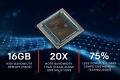
용량 데이터 세트를 처리할 경우, 대역폭은 매 단계마다 작업 속도에 영향을 미친다. 보안 처리, 빅 데이터 분석, 데이터베이스 가속, 비디오 트랜스코딩과 같은 데이터 집약적 작업부하의 경우, 성능을 향상시키기 위해선 많은 HBM 용량이 필요하다. 자일링스가 새로 개발한 16GB 버텍스 울트라스케일+ HBM FPGA는 메모리 대역폭이 460GB/s으로 DDR4 DIMM보다 20배 더 크며 전력소모는 75% 수준이다.
2019-09-24 오후 1:30:12by 이수민 기자
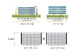
삼성전자가 12단 3차원 실리콘 관통전극(3D-TSV) 기술을 개발했다. 12단 3D-TSV는 금선을 이용해 칩을 연결하는 대신 반도체 칩 상단과 하단에 머리카락 굵기의 1/20 수준인 수 마이크로미터 직경의 TSV 6만개를 만들어 연결하는 패키징 기술이다. 종이의 절반 이하 두께로 가공한 D램 칩 12개를 적층해 수직으로 연결해 기존 와이어 본딩 기술보다 칩들 간 신호를 주고받는 시간이 짧아져 속도와 소비전력을 개선할 수 있다.
2019-10-07 오전 10:01:21by 이수민 기자

.jpg)

[열린보도원칙] 당 매체는 독자와 취재원 등 뉴스이용자의 권리 보장을 위해 반론이나 정정보도, 추후보도를 요청할 수 있는 창구를 열어두고 있음을 알려드립니다.
고충처리인 장은성 070-4699-5321 , news@e4ds.com