인피니언 6월23일부터
Physical AI HBM Smart Factory SDV AIoT Power Semicon 특수 가스 정정·반론보도 모음 e4ds plus

​Saenggiwon, first domestic production of high-flatness semiconductor copper plating solution

Google 우선 소스 기사입력2021.09.03 09:30

The source of life and the plating thickness deviation are within 2%
Development of high flatness semiconductor copper plating solution
Transfer technology to domestic companies and launch products


On the 31st, the Korea Institute of Industrial Technology (KITECH) independently developed the original technology for a high-flatness ‘copper plating solution’ for semiconductors and, together with a technology transfer company, launched the product, achieving its first domestic production.
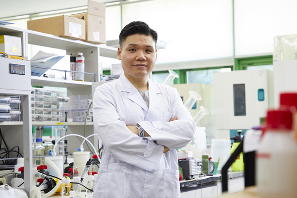
▲ Developed a copper plating solution technology for high-flatness semiconductors
Dr. Lee Min-hyung, Korea Institute of Industrial Technology [Photo = Korea Institute of Industrial Technology]

Copper plating solution is mainly used in the 'bumping' process, which involves plating the circuit pattern on the wafer with copper to give only that part electrical properties. It is the only material with a 'zero (0%) domestic production rate' among all semiconductor processes, relying entirely on imports from Japan and the United States.

The research team led by Dr. Lee Min-hyung of the Eco-friendly Thermal Surface Treatment Research Division of Saenggiwon conducted approximately 15,000 experiments over three years to find the optimal additive and mixing ratio among various organic additives that can adjust the flatness of the plating film surface, and achieved high flatness within a plating thickness deviation of 2%.

Usually, after plating, the surface becomes convex like a water droplet, but the flatter it is, the more evenly the current is transmitted, improving the production yield and the performance of the final product. The developed plating solution was implemented by deriving and mixing the ratio of two additives, a ‘convex shape inducer’ and a ‘concave shape inducer’, based on the principle of theorem synthesis, which states that when a convex shape and a concave shape are combined, they become flat.

As a result of the process test at the demand company, it was shown that high flatness with a plating thickness deviation of 'within 2%' was secured at a high-speed plating speed of up to 3 micrometers (㎛) per minute, which improved productivity by approximately 150% compared to existing imported materials. In addition, by databased the results of numerous additive mixing experiments accumulated so far, another advantage is that customized plating solutions with upward convex or downward concave characteristics can be produced as desired by the demand company.

The research team transferred the technology to a domestic electronic materials company and launched the product in December of last year. It has been tested and evaluated in the semiconductor manufacturing process of a large company for the past six months. The transferred technology was developed considering all plating conditions and variables based on the premise of ‘mass production’, so it took only eight months from technology transfer to product launch and large company test evaluation.

Currently, we have received feedback from the relevant large company that it satisfies all the plating characteristics required for 12-inch large wafers and next-generation semiconductor products. If the evaluation is successfully completed within a few months, the first domestic production of plating materials and equipment used in approximately 80% of domestic semiconductor production products will be achieved, and reverse exports to Japan and other countries are also expected to be possible.

Dr. Lee Min-hyung of Saenggiwon said, “The semiconductor plating solution market, which is worth about 200 billion won, is a small field for large companies to enter, and it requires advanced technologies for small and medium-sized companies, so domestic production has been slow,” and added, “Following the development of through-silicon via (TSV) products for implementing 3D integrated circuits, we plan to research high-performance tin-silver and indium plating solutions that can be utilized in various industries.”
이수민 기자
기사 전체보기