삼성전자, 차세대 반도체 패키징 기술로 업계 선도
기사입력 2021.11.11 08:58
2.5D 패키징 솔루션 ‘H-Cube’ 개발
이종 기판 사용 고성능·대면적 구현
이종 기판 사용 고성능·대면적 구현
삼성전자가 차세대 반도체 패키징 기술로 고성능 반도체 공급을 확대한다.
삼성전자는 반도체 패키징 기술 혁신을 통해 고성능 반도체용 2.5D 패키징 솔루션 ‘H-Cube(Hybrid-Substrate Cube)’를 개발했다고 11일 밝혔다.
삼성전자는 기존 2.5D 패키징 솔루션 I-Cube에 이어 이번에 고대역폭 메모리(HBM)를 6개 이상 탑재 가능한 업계 최고 사양의 ‘H-Cube’를 확보하며, 데이터센터·AI·네트워크 등 응용처별 시장에 맞는 맞춤형 반도체를 고객의 니즈에 맞춰 다양한 형태의 패키지로 제공할 수 있게 됐다.
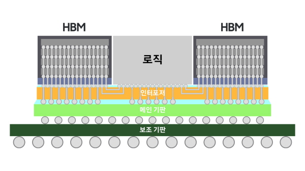
삼성전자 ‘H-Cube’는 실리콘 인터포저 위에 CPU, GPU 등의 로직(Logic)과 HBM을 배치한 2.5D 패키징 솔루션으로, HPC, 데이터센터, 네트워크용 고사양 반도체에 사용된다.
‘H-Cube’는 고사양 특성 구현이 용이한 메인 기판 아래, 대면적 구현이 가능한 보조 기판을 추가로 사용하는 2단 하이브리드 패키징 구조로, 로직과 함께 HBM 6개 이상을 효율적으로 탑재 가능한 장점이 있다.
삼성전자는 메인 기판과 보조 기판을 전기적으로 연결하는 솔더볼(Solder ball)의 간격을 기존 대비 35% 좁혀 기판의 크기를 최소화하며, 다수의 HBM 탑재로 인하여 증가하는 대면적 기판 제작의 어려움을 극복했다.
또한 메인 기판 아래 보조 기판을 추가해 시스템 보드와의 연결성을 확보했다.
삼성전자는 다수의 로직과 HBM을 적층하면서도 칩에 안정적인 전원을 공급하고 신호의 손실이나 왜곡을 최소화 할 수 있도록 칩 분석 기술도 적용하여 이번 솔루션의 신뢰도를 높였다.
삼성전자 파운드리사업부 마켓전략팀 강문수 전무는 “‘H-Cube’는 삼성전자와 앰코테크놀로지, 삼성전기가 오랫동안 협력해온 결과로 많은 수의 칩을 집적해야하는 고사양 반도체를 위한 최적의 솔루션”이라며 “삼성전자는 앞으로도 파운드리 파트너와의 긴밀한 협력을 통해 기술적 한계를 넘어서는 다양한 패키징 솔루션을 제공해 나갈 것”이라고 밝혔다.
앰코테크놀로지 기술연구소 김진영 상무는 “삼성전자와 앰코테크놀로지가 H-Cube 솔루션을 성공적으로 개발하며 HPC, AI 시장에서 요구되는 반도체 집적 기술 구현의 난관을 극복했다”며 “파운드리와 OSAT(반도체 패키징, 테스트 전문업체)의 협업 관계를 성공적으로 이루어 낸 것에 큰 의미가 있다”고 말했다.

관련뉴스
-

반도체 패키징 소재 분야, 연평균 3.4% 성장 전망
SEMI는 전자산업 전문 조사기관 테크서치의 최신 글로벌 반도체 패키징 소재 전망 보고서를 인용하며 반도체 패키징 재료 시장 규모가 2019년 176억 달러에서 2024년 208억 달러까지 성장하며 연평균 성장률 3.4%를 기록할 것으로 전망된다고 밝혔다.
2020-07-29 오전 10:22:39by 강정규 기자
-

반도체 2.5D 패키징의 중요성, 공정 미세화를 뛰어넘다
2.5D 및 3D 집적 기술은 첨단 반도체의 수율 문제 해결을 위해 고안됐다. 그리고 그 효용은 TSMC가 자일링스의 FPGA를 CoWoS 기술로 양산함으로서 입증했다. 이에 착안한 인텔은 포베로스 기술을 개발하여 자사의 CPU 성능을 높였다. 국내 시스템 반도체 산업이 TSMC와 인텔을 극복하려면 기존의 패키징 기술에 대한 관점을 부정하는 파괴적인 혁신이 필요하다.
2020-09-15 오후 4:21:12by 이수민 기자
-

고성능 반도체 수요 늘며 후공정 '패키징' 중요성 커져
대표적인 반도체 후공정인 패키징 공정은 전공정에서 제작된 소자를 포장하여 완성품으로 제작하는 과정이다. 업계에선 소자의 고집적 및 다기능 구현을 위한 핵심 기술로 주목하고 있다. 여러 소자를 하나로 통합하는 첨단 패키징 기술은 전기적 연결과 반도체 소자 보호가 목적인 전통적인 패키징 기술을 대체하고 있다.
2021-09-13 오후 4:40:51by 이수민 기자

.jpg)
많이 본 뉴스
[열린보도원칙] 당 매체는 독자와 취재원 등 뉴스이용자의 권리 보장을 위해 반론이나 정정보도, 추후보도를 요청할 수 있는 창구를 열어두고 있음을 알려드립니다.
고충처리인 장은성 070-4699-5321 , news@e4ds.com