[연재]ST 유지 카와노 엔지니어⑨-GPIO, MCU 입출력 핵심
기사입력 2021.12.07 10:28
GPIO, MCU 입출력 핵심
GPIO, STM32·STM8 MCU I/O 포트
다양한 애플리케이션 및 용도로 사용
[편집자주]일반적으로 반도체라 하면 컴퓨터의 CPU와 메모리처럼 일반인에게 익숙한 반도체를 떠올리기 마련이다. 반면에 전자제품 구동을 위해서 핵심 반도체로 쓰이는 MCU(Micro Controller Unit)의 경우 일반적으로 우리가 쉽게 접하는 모든 전자제품에서 사용되고 있으면서도 일반인에게는 아직 낯선 반도체다. 이런 MCU가 최근 반도체 부족 사태로 인해 언론에 오르내리며, 일반인들에게 주목받기 시작했다. 이에 본지는 MCU 반도체 전문기업인 ST마이크로일렉트로닉스의 유지 카와노 매니저의 연재기고를 통해 MCU에 대해 전문적으로 알아보는 자리를 마련했다.
.jpg) ■ 바이너리 신호 입출력하는 MCU
■ 바이너리 신호 입출력하는 MCUMCU가 수행하는 가장 단순한 작업은 포트를 통해 바이너리(0/1) 신호들을 출력하는 것과 포트로부터 바이너리 신호들을 읽어 들이는 것이다. 매우 간단하지만, 이들 기능들은 필수이며 모든 고성능 MCU가 채용하고 있다. 본고에서는 이러한 기능들을 수행하는 디바이스와 입력/출력 포트에 대해 설명한다.
■ IO, 바이너리 신호 읽는 부품
입력/출력 포트는 바이너리 신호를 포트를 통해 출력하고 포트로부터 입력되는 바이너리 신호들을 읽는 부품으로 일반적으로 정의된다. 이와 같은 포트들은 IO(또는 I/O) 포트라고도 한다. ST마이크로일렉트로닉스(이하 ST)가 생산하는 STM32 및 STM8 MCU의 I/O 포트는 GPIO(general-purpose input/output pin)라고 하는 데, 다양한 애플리케이션과 용도를 위해 사용되기 때문이다. ‘포트’라는 단어는 확실히 화물이 선적되고 출하되는 항구라고도 할 수 있다. MCU가 처리하는 ‘화물’이 0과 1로 구성된 데이터 조각이라는 점을 제외하면 이것은 MCU에 의해 수행되는 역할에 대한 적절한 비유라고 할 수 있다.
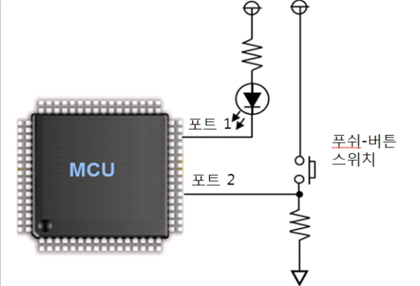
▲그림 1 : GPIO의 역할
그림 1은 GPIO에 대한 가장 간단한 애플리케이션 중 하나이다. 푸쉬-버튼 스위치가 꺼졌을 경우, ‘0’(접지 레벨)이 포트2에 입력된다. 버튼을 누르면 입력이 ‘1(전력공급 전압 레벨)’로 변환하다. 하지만, 포트 1이 일반적으로 ‘1’을 출력하면, 결과적으로 LED가 턴-오프 상태를 유지하며, ‘0’을 출력하면 LED가 온 상태로 전환된다.
이러한 기능들은 MCU 프로그램과 연결되어 있으며, 버튼을 누르면 LED를 온 상태로 전환하고, 버튼을 누르지 않으면 오프 상태로 전환한다.
이 포트가 실제로 어떻게 사용되는지 예를 들면, 푸쉬-버튼 스위치를 제어 회로 입력 신호로 대체하고 LED를 모터-드라이버 IC로 대체할 수 있다.
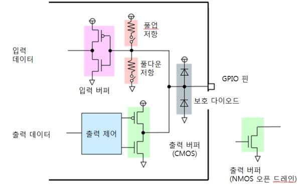
▲그림 2 : GPIO의 구조
다음은 GPIO의 내부 구조에 대해 살펴보자. MCU 구조는 제조업체에 따라 다르기 때문에, 특정 MCU의 구조에 대한 자세한 설명은 관련 사용 설명서를 읽을 필요가 있다. 예를 들어, STM32의 GPIO 구조를 살펴보자.
그림 2는 GPIO의 구조 다이어그램을 보여준다. 위 부분은 입력 회로이며, 아래 부분은 출력 회로이다. 우측은 데이터가 들어가고 나오는 GPIO 핀이다. 이 핀 바로 다음에는 전원 또는 접지에 대해 노이즈와 서지 전압(surge voltage)을 방지하는 보호 다이오드가 위치한다. GPIO는 풀업/풀다운 저항을 가지고 있기 때문에 필요한 외부 저항의 수를 줄일 수 있다. 소프트웨어는 이러한 풀업/풀다운 저항을 회로에 연결하거나 차단할 수 있다. CMOS 회로는 입력 데이터를 받아들여 내부 회로에 전달한다. 이 CMOS 회로는 입력 버퍼로 지칭된다. 이 다이어그램에서는 CMOS 인버터가 버퍼로 사용된다.
MCU로부터 출력되는 데이터는 출력 버퍼를 통해 전송된다. 이 버퍼는 CMOS 인버터로 구성되며, MCU 외부에 있는 회로들을 구동하기 위해서 높은 구동 성능을 가진 CMOS를 사용한다.
GPIO 구조의 한 형태는 NMOS 드레인이 오픈 상태를 유지하는, 즉 PMOS가 NMOS에 연결되지 않는 NMOS 오픈-드레인(open-drain) 구조이다.
단지 NMOS만으로(즉, PMOS 없이) 구성된 출력 버퍼를 NMOS 오픈-드레인이라고 한다. 참고로 그림 2의 우측에 이러한 형태의 드레인을 나타냈다. 이 버퍼는 외부 풀업 저항을 필요로 하는데 '1'(high)를 자체적으로 출력할 수 없기 때문이다. 예를 들면, I2C 통신 포트에 대해 NMOS 오픈-드레인 구조를 사용한다.
사실상 전기 신호들이 GPIO 회로의 입력이기 때문에, 푸쉬-버튼 회로를 만들고자 할 경우에 어떤 전압이 ‘0’으로 표현되고 어떤 전압이 ‘1’로 표현되는지를 알아야 한다. MCU와 같은 디지털 로직 회로의 경우, “0”과 ‘1’을 나타내는 2개의 전압 범위 사이의 경계선 레벨을 쓰레스홀드(threshold) 레벨이라고 한다. CMOS 회로는 MCU 내부 회로에서 신호를 수신하기 때문에, 쓰레스홀드 레벨은 CMOS를 구성하는 PMOS/NMOS 회로를 온 또는 오프 상태로 전환하는 전압이다.
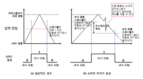
▲그림 3 : 쓰레스홀드 값
이제 그림 3(a)를 살펴보자. GPIO에 대한 입력 전압을 전원 공급 레벨에 도달할 때까지 GND(0V)로부터 점진적으로 증가시킨 다음, 다시 이를 점진적으로 낮춘다고 가정해 보자. 초기에 GPIO는 입력 전압을 ‘0’으로 인식하지만, 일단 특정 전압을 초과하게 되면 GPIO는 이것을 ‘1’로 인식한다. 앞서 언급한 바와 같이 이러한 경계 전압을 문턱 전압(threshold voltage)이라고 한다. 출력 전압이 문턱 전압 이하로 낮아질 경우, GPIO는 이것을 다시 ‘0’으로 인식한다.
노이즈가 많은 입력 신호에도 불구하고 안정적으로 동작할 수 있도록 하기 위해서 2개의 쓰레스홀드 레벨을 가지는 또 다른 형태의 GPIO가 있다. 한 개의 쓰레스홀드는 ‘0’에서 ‘1’로 전환할 때를 위한 것이고, 다른 하나는 ‘1’에서 ‘0’으로 전환할 때를 위한 것이다. 2개의 쓰레스홀드를 사용하는 GPIO를 슈미트-트리거(Schmitt-trigger) 특성을 가지고 있다고 말한다.
다음으로 그림 3(b)를 살펴보자. 이 그림은 그림 3(a)와 다르다. ‘0’에서 ‘1’로 전환 시의 쓰레스홀드가 ‘1’에서 ‘0’으로 전환 시와 동일하지 않다. 이들 2개의 쓰레스홀드 레벨 사이의 전압 차이를 히스테리시스 전압(hysteresis voltage) 범위라고 한다.
일단 GPIO가 전압 레벨을 ‘1’ 또는 ‘0’으로 인식하면, 노이즈가 있는 경우일지라도 전압 레벨이 히스테리시스 전압 범위 내에서 변동하는 한 입력 레벨에서의 변동을 인식하지 않는다. 다시 말해, 노이즈 내성이 있다.
이러한 형태의 GPIO는 통신, 리셋 포트, 인터럽트 요청 포트 등을 위한 클록 입력 포트에 사용되며, 노이즈-유도 에러(전압 변동 및 채터링 포함)를 방지한다
각기 다른 MCU는 입력 특성에 대해 각기 다른 조건을 사용하지만, 일반적으로 VIH라고 하는 것은 H-쓰레스홀드를, VIL은 L-쓰레스홀드를 나타낸다.
■ 출력이 ‘1’이 아니거나 ‘0’도 아닌 환경이 있다는 것 주의해야
.jpg)
▲그림 4 : 출력 특성
일반적으로 VOH는 ‘1’의 출력 전압을 나타내고, VOL은 ‘0’의 출력 전압을 나타낸다. 출력 버퍼 MOS의 특성은 이들 전압에 영향을 미친다. 그림 4를 살펴보자. ‘1’이 출력일 경우(그림 4(a)), PMOS는 온 상태로 전환되고, ‘0’이 출력일 경우(그림 4(b), NMOS가 온 상태로 전환된다. 전자의 경우, PMOS에 나타나는 전압 강하(그림 4의 Vpmos)로 인해 출력 전압이 전원 전압(Vdd)과 다소 차이가 발생하게 된다. 후자의 경우, NMOS에 나타나는 전압 강하(그림 4의 Vnmos)로 인해 출력 전압이 GND 레벨(Vss)과 다소 차이가 발생하게 된다. 결과적으로 출력 전압은 다음과 같다. VOH = Vdd - Vpmos 및 VOL = Vss + Vnmos. 특정 값에 대해서는 관련 MCU의 전기적 특성들을 명시하고 있는 매뉴얼을 참고하면 된다.
출력이 ‘1’이 아니거나 ‘0’도 아닌 환경이 있다는 것을 주의해야 한다. PMOS와 NMOS가 모두 오프 상태일 경우에 발생하는 이 상태를 ‘고 임피던스(high impedance) 상태’, ‘오픈 상태’ 또는 ‘3상태(tri-state)’라고 하고, ‘H-Z’ 또는 ‘High-Z’로 표시한다. 고 임피던스는 출력 상태가 전원공급 또는 GND와 관련해서 높은 임피던스를 가지고 있다는 것을 의미한다. 이 출력 특성은 H와 L의 두 상태 이외의 제3의 상태이기 때문에, 그것을 ‘3-상태’라고 한다. ‘오픈 상태’라는 것은 출력 회로가 어떠한 것과도 연결되어 있지 않다는 것을 의미한다.
관련뉴스
-
.jpg)
[연재]ST 유지 카와노 엔지니어⑥-다양한 연산작업 ALU, MCU ‘핵심부’
MCU는 CPU나 GPU와 다르게 낯설지만, 가장 많이 사용되는 반도체 중 하나다. ST 시스템 솔루션 랩의 유지 카와노 매니저에게 MCU의 활용성과 가능성이 얼마나 큰지 들어보자.
2021-10-25 오후 5:47:30by 편집부
-
.jpg)
[연재]ST 유지 카와노 엔지니어⑦-MCU의 언어, ‘C’
MCU는 CPU나 GPU와 다르게 낯설지만, 가장 많이 사용되는 반도체 중 하나다. ST 시스템 솔루션 랩의 유지 카와노 매니저에게 MCU의 활용성과 가능성이 얼마나 큰지 들어보자.
2021-11-09 오후 2:02:47by 편집부
-

[연재]ST 유지 카와노 엔지니어⑧-MCU 연결 툴 선택, 용도·콘텐츠 따라서 결정
MCU는 CPU나 GPU와 다르게 낯설지만, 가장 많이 사용되는 반도체 중 하나다. ST 시스템 솔루션 랩의 유지 카와노 매니저에게 MCU의 활용성과 가능성이 얼마나 큰지 들어보자.
2021-11-15 오전 10:53:29by 편집부

.jpg)

많이 본 뉴스
[열린보도원칙] 당 매체는 독자와 취재원 등 뉴스이용자의 권리 보장을 위해 반론이나 정정보도, 추후보도를 요청할 수 있는 창구를 열어두고 있음을 알려드립니다.
고충처리인 장은성 070-4699-5321 , news@e4ds.com