.jpg)
▲이상민 웨이비스 연구소장
이상민 웨이비스 연구소장, “패키지에서 완제품까지 GaN 솔루션 보유”
0.3-4㎛소자 솔루션 보유, 0.1-2㎛ 내년도 서비스해 RF·증폭기 등 활용
차세대 반도체 소자로 손꼽히는 갈륨 나이트라이드(GaN) 반도체는 저전력 솔루션의 핵심으로 전력 효율이 높고 더 높은 주파수, 전압, 온도에서 낮은 전력 손실로 작동이 가능해 관련 시장이 점차 확대되고 있는 추세이다.
이러한 GaN 반도체 기술로 RF 소자를 만들어 5G·6G 이동 통신과 위성통신, 군수 레이더에 사용되는 GaN RF 소자를 생산하는 기업이 있다. 국내 반도체 기업 웨이비스가 국내 최초로 GaN RF 반도체 팹을 보유해 관련 제품 설계와 생산 솔루션 서비스를 제공하고 있다.
한국전자파학회 학계학술대회 산업체 전시회에서 이상민 웨이비스 파운드리사업부 연구소장을 만나 이야기를 나눠봤다.
■ 웨이비스 소개를 부탁드린다
2017년 창업한 웨이비스는 국내 유일한 GaN 전자 소자를 제작하는 파운드리를 가지고 있는 유일한 회사이다.
■ 마이크로미터 단위는 무엇을 의미하는가?
웨이비스 파운드리 공정을 0.1~0.4㎛(마이크로미터)로 표시했는데 이는 갈륨 나이트라이드 소재의 게이트 길이를 의미한다. 그래서 게이트 길이가 짧아질수록 주파수는 높아진다.
■ 어떤 솔루션을 가지고 있나?
웨이비스는 2018년부터 0.4㎛ 양산에 들어갔으며 0.3㎛ 소자는 2019년부터 시작했다. 0.2㎛ 공정은 현재 개발 중에 있다. 아직 신뢰성 시험을 준비하는 중에 있으며 0.1㎛대 소자도 현재 단위 공정을 개발해서 내년에 본격 개발을 진행할 계획이다.
0.4㎛ 소자는 S대역(S-Band)이라고 부르는 4G(LTE) 신호 대역과 5G 낮은 주파수 영역에서 응용이 가능하며 현재 이러한 소자들은 군 무기체계인 레이더에 적용되고 있다.
0.3㎛ 소자는 C대역(C-Band)에 속하는 4~8GHz 주파수를 커버할 수 있으며 0.2㎛ 소자는 X대역(X-Band)과 Ku대역(K under Band)인 8~18GHz 주파수를 커버할 수 있다.
0.1㎛ 소자는 Ka대역(Ka-Band) 24~36GHz를 커버할 수 있는 고주파 RF소자이다.
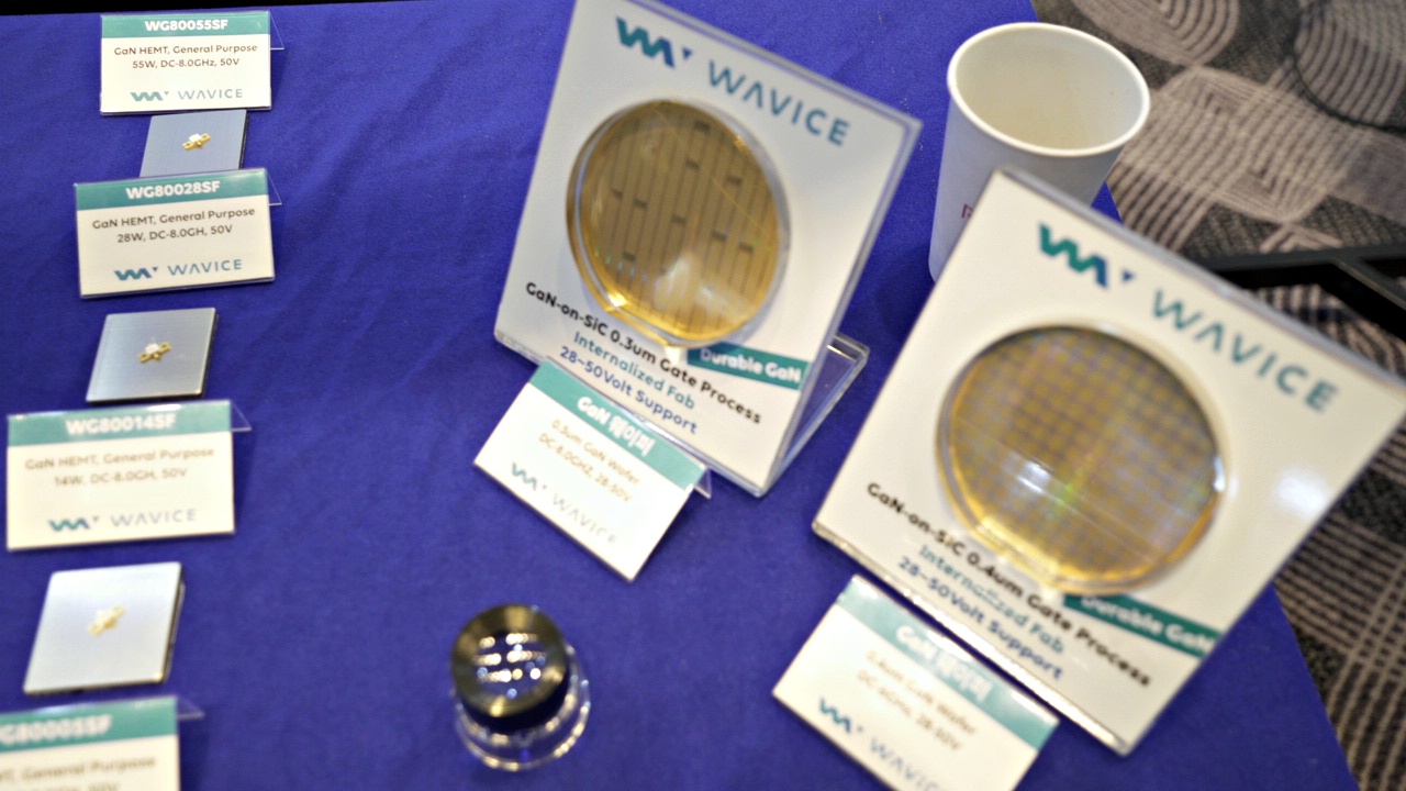
▲웨이비스 4인치 GaN 웨이퍼 샘플
4인치 웨이퍼에서 GaN 소자를 생산하는 파운드리 사업부와 제작된 소자를 패키지 TR과 RF 모듈을 만드는 2가지 사업부로 이뤄져 있다. 파운드리를 원하는 고객들은 파운드리 사업부에서 서비스를 받을 수 있으며, 패키징에서 완제품까지 원하는 경우에는 작은 패키지 트랜지스터를 만들어서 받아볼 수 있다.
세라믹 패키지 안에 GaN소자가 들어 있으며 이러한 소자들을 모듈형태로 회로와 함께 구성하게 되면 굉장히 큰 SSPA(Solid State Power Amplifier)와 같은 Power Amplifier까지도 서비스 받을 수 있다.
웨이비스는 창사한 지 5년 정도이나 국내에서는 유일하게 GaN 소자를 파운드리를 통해 제작이 가능하며 그것을 이용해 RF완제품과 증폭기 생산 등을 현재 서비스하고 있다.
감사합니다.