“MOSFET 선택, 파라미터 차이 전류 분배 고려 必”
전류 불평형 높을수록 한쪽 MOSFET으로 더 높은 손실 누적
인피니언, 낮은 RDS(on) 값 그대로 유지 전류공유 향상 설계
■ 전류 불평형 시 모스펫간 전력 소모 불균형
모터 드라이브 애플리케이션은 하프 브리지 토폴로지(통상적으로 3상)를 사용해서 AC 전력 신호를 발생시키고 이것을 사용해서 전기 모터로 양 또는 음의 토크를 발생시킨다. 이때 각기 스위치로 병렬
MOSFET을 사용해서 높은 출력 전류를 달성할 수 있다.
MOSFET을 병렬로 사용할 때는 병렬 디바이스들 간에 전류 분배를 고려해야 한다. 레이아웃 비대칭이나 MOSFET 파라미터 차이 등으로 인해서 전류 불평형이 발생되면 MOSFET들 간에 전력 소모가 불균형해질 수 있다.
이 글에서는 MOSFET 파라미터 차이가 병렬 MOSFET들 간에 전류 불평형에 어떻게 영향을 미치고 그로 인해서 평균 전력 소모 불평형에는 어떻게 영향을 미치는지 살펴본다. 전력 소모와 시스템 성능을 이해하기 위해서는 레이아웃과 스위칭에서부터 부하 전류와 PWM 방식에 이르는 다양한 시스템 특성들을 고려해야 한다. 이러한 분석은 애플리케이션이나 시스템에 따라서 약간씩 차이는 있을 수 있으나 기본적으로 동일하게 적용할 수 있다.
또한 이 글에서는 병렬 MOSFET들 간에 VGS(th)를 일치시키는 것의 중요성과 트랜스컨덕턴스(gfs)가 전류 공유에 미치는 영향에 대해서 설명한다. gfs가 낮으면 병렬 MOSFET들 간에 전류 평형을 향상시킬 수 있으나, 높은 RDS(on) 값을 수반한다는 점에 있어서 전도 특성 또한 고려해야 한다.
■ AC 출력 부하 전류일 때 MOSFET 전력 소모 계산
MOSFET 파라미터가 결과적인 총 전력 소모에 미치는 영향을 이해하기 위해서 상측과 하측 모두 2개 MOSFET을 병렬로 연결한 하프 브리지를 사용해서 시뮬레이션을 실시했다. 그림 1의 회로 모델은 완벽하게 대칭적이도록 단순화한 것이다. 하지만 각기 회로로 트레이스들의 기생 인덕턴스와 저항을 고려해야 한다. MOSFET Q1과 Q3이 병렬로 상측 스위치를 형성한다.
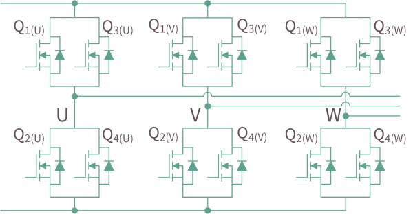
▲그림 1 : 각기 스위치로 병렬로 2개 MOSFET을 사용한 3상 인버터
시스템 전력 소모를 분석하기 위해서는 순간 전력 소모와 평균 전력 소모를 구분해야 한다. 순간 전력 소모는 극히 동적인 요소이다. MOSFET 전력 소모는 다음과 같은 요소들로 이뤄진다.
· EON - MOSFET switching loss at turn-on
· EOFF - MOSFET switching loss at turn-off
· PCND - conduction loss of the open MOSFET channel in forward conduction
· PD - conduction loss of the body diode
· EDoff - reverse recovery loss of the body diode
· EON - 턴온 시에 MOSFET 스위칭 손실
· EOFF - 턴오프 시에 MOSFET 스위칭 손실
· PCND - 순방향 전도 시에 개방 MOSFET 채널의 전도 손실
· PD - 바디 다이오드의 전도 손실
· EDoff - 바디 다이오드의 역 복구 손실
이들 각각의 요소가 전반적인 전력 소모에 미치는 영향은 부하 전류 특성과 사용하는 제어 방식에 따라서 크게 좌우된다. 그러므로 주어진 애플리케이션으로 적합한 방식으로 특정한 MOSFET 파라미터가 전반적인 시스템 성능에 어떻게 영향을 미치는지 고려해야 한다.
평균 전력 소모와 열 특성이 디바이스 온도를 결정하므로 시스템 성능에 있어서 직접적인 제한 요소이다. 평균 전력 소모는 스위칭 손실과 전도 손실을 합친 것이라고 할 수 있다.
· PQ1-SW(avg) - average switching losses at MOSFET Q1
· PQ1-CND(avg) - average conduction losses at MOSFET Q1
· PQ1-TOT(avg) - total average losses at MOSFET Q1 (sum of PQ1-CND(avg) and PQ1-SW(avg))
· PQ1-SW(avg) - MOSFET Q1의 평균 스위칭 손실
· PQ1-CND(avg) - MOSFET Q1의 평균 전도 손실
· PQ1-TOT(avg) - MOSFET Q1의 총 평균 전력 소모(PQ1-CND(avg)와 PQ1-SW(avg)의 합)
DC 출력 전류를 사용하는 비교적 단순한 조건으로는 단일 PWM 사이클만을 사용해서 정상 상태(steady-state) 동작으로 평균 전력 소모를 계산할 수 있다. 하지만 사인파 출력 전류로 전력 소모를 계산하기 위해서는 최소한 하나의 전체적인 사인파 사이클을 고려해야 한다. 각기 PWM 사이클로 전류 진폭이 다르기 때문이다.
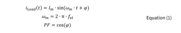
이 글에서는 하프 브리지 출력으로서 AC 부하 전류를 사용할 때의 MOSFET 전력 소모에 대해서 설명하고 있다. 대부분의 모터 드라이브 애플리케이션이 그렇기 때문이다. 그러므로 출력 부하 전류는 다음 공식에 따라서 특정한 진폭의 사인파이다.
스위칭 변조 방식은 SPWM(sinusoidally-weighted pulse width modulation)이고, 표 1에서와 같은 조건과 설정을 사용한다. 이 글에서 언급하는 모든 사례들로 동일한 SPWM 조건을 사용한다.
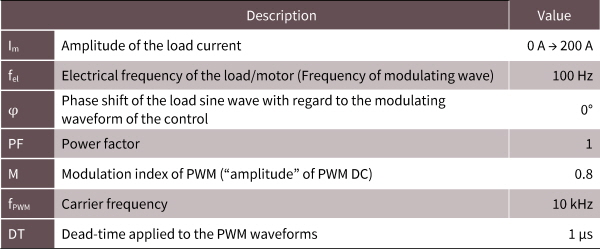
▲표 1 : 부하 조건과 SPWM 파라미터
병렬 MOSFET들 간에 불평형과 관련해서, 신뢰할 수 있는 시스템 디자인을 달성하기 위해서는 각기 MOSFET의 전력 소모를 고려해야 한다. 그러므로 이 글에서는 각기 다른 조건으로 개별 MOSFET으로 출력 부하 전류에 따른 평균 전력 소모를 보여준다.
이 결과를 해석할 때 가장 중요한 것은 어느 MOSFET이 더 많은 전력을 소모하느냐 하는 것이다. 이 MOSFET(‘가장 뜨거운’ MOSFET)이 시스템 출력 전류에 있어서 병목 지점으로 작용한다.
MOSFET 파라미터마다 다양한 방식으로 전류 공유에 영향을 미친다. RDS(on)은 MOSFET 전도 시에 영향을 미치며, 또 다른 파라미터들(VGS(th), RG, CGS, CGD)은 스위칭 시에 전류 공유에 영향을 미친다. 완벽하게 대칭적인 레이아웃으로 시뮬레이션을 실시함으로써 개별 MOSFET 파라미터들이 미치는 영향을 살펴볼 수 있다.
다른 파라미터들에 비해서 VGS(th) 차이가 전반적인 성능에 더 중요하게 영향을 미치는데, VGS(th) 차이는 통상적인 MOSFET 제조 과정에서 발생되는 차이 때문이다. VGS(th) 차이는 전력 소모에 있어서 불평형으로 이어진다. 병렬 MOSFET들 간에 VGS(th)가 낮은 MOSFET이 턴온과 턴오프 둘 다로 스위칭 손실이 증가한다. 이것이 다른 파라미터들과 다른 점이다. 뿐만 아니라 VGS(th)는 온도에 대한 종속성이 음이라서 이 점이 불평형을 가중시킨다. 다만 이 글에서는 온도 종속성에 대한 논의는 배제시켰다.
병렬 MOSFET들 간에 VGS(th) 일치의 중요성을 보여주는 것으로서, 그림 2의 그래프들은 두 가지 VGS(th) 차이 조건으로 MOSFET 전력 소모를 비교해서 보여준다.
표 2에서는 시뮬레이션에 사용된 VGS(th) 값들을 보여준다.
그림 2에서 주황색 선은 VGS(th)가 데이터 시트에서 표기하고 있는 최대 값과 최소 값으로서 VGS(th) 차이가 최악 상황일 때의 결과를 보여준다. 주어진 출력 전압으로 Q1의 전력 소모가 Q3의 전력 소모보다 거의 두 배까지 달한다는 것을 알 수 있다.
통계적으로 이와 같은 극단적인 차이는 가능성이 거의 희박할 것이다. 그러므로 샘플 로트의 파라미터 분포를 고려해서 좀 더 현실적인 조건을 살펴볼 필요가 있다. 그림 2에서 초록색 선은 VGS(th) 차이가 ∆VGS(th) = 0.5V로 좀 더 낮을 때의 결과를 보여준다.
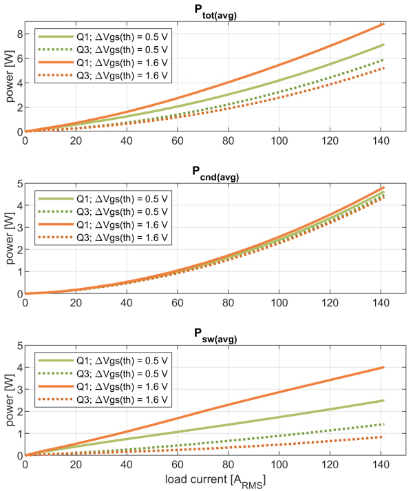
▲그림 2 : MOSFET Q1과 Q3(병렬로 2개 MOSFET)으로 평균 전력 소모
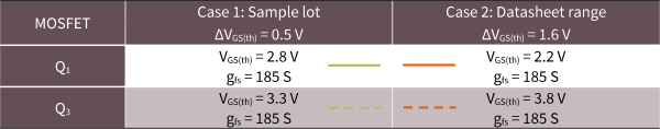
▲표 2 : MOSFET 파라미터 - VGS(th) 차이
전력 소모는 MOSFET 평균 온도에 비례하며 그러므로 시스템 출력 전류의 한계를 결정한다. 어떠한 MOSFET으로든 최대 디바이스 온도를 넘지 않아야 하기 때문이다.
시스템 크기를 축소하기 위해서는 MOSFET을 병렬로 사용할 때 전류 불평형을 낮추는 것이 중요하다. 전류 불평형이 높으면 어느 한 디바이스로 전력 소모가 집중됨으로써 병렬화의 이점을 사라지게 할 것이다.
그러므로 병렬로 사용하기 위한 MOSFET을 선택할 때는 생산 시의 VGS(th) 차이가 크지 않은 MOSFET을 선택하는 것이 중요하다.
■ 트랜스컨덕턴스(gfs)가 전류 공유에 미치는 영향
스위칭 시에 전류 불평형은 ∆VGS(th)에 의해서 크게 영향을 받는다. 하지만 불평형에 영향을 미치는 것은 이뿐만 아니다. 각기 다른 트랜스컨덕턴스(gfs) 값으로 VGS(th)의 영향을 살펴보면 전류 공유에 미치는 영향을 좀 더 잘 이해할 수 있다. gfs 값은 ID 범위에 걸쳐서 일정하지 않다. 그림 3은 이 특성을 보여준다. 데이터 시트에서 gfs(예를 들어서 gfs = 185)는 통상적으로 특정한 ID일 때의 값으로 표기된다. 그러므로 정확한 시뮬레이션을 위해서는 전체적인 범위에 걸쳐서 이 특성을 고려해야 한다.
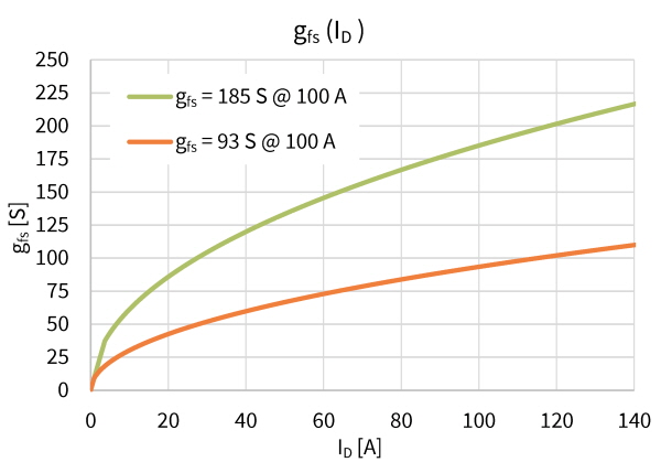
▲그림 3 : OptiMOS™ 기술로 ID에 따른 gfs
gfs를 낮추는 것은 스위칭 손실과 전도 손실 모두에 영향을 미친다. RDS(on)은 gfs와 상관적이므로, gfs가 낮은 MOSFET을 선택하면 전도 손실이 증가한다. 낮은 gfs는 또한 스위칭을 늦추므로 스위칭 손실을 증가시킨다.
공정한 비교를 위해서 표 3에서는 각기 다른 gfs 값으로 RG 네트워크를 통해서 스위칭 속도(스위칭 시의 diD/dt)를 매칭시켰다.
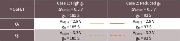
▲표 3 : MOSFET 파라미터 - ∆VGS(th) = 0.5V로 gfs를 낮춤
그림 4에서는 Q1과 Q3 사이에 VGS(th) 차이 ∆VGS(th) = 0.5V로 두 가지 gfs 값을 비교해서 보여준다. 스위칭 시에 diD/dt를 매칭시키기 위해서 낮은 gfs로 Rg 값을 낮췄다.
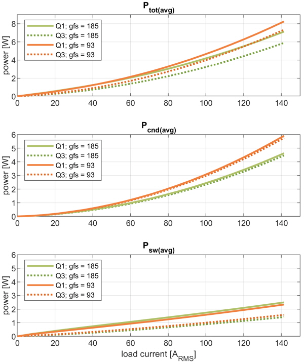
▲그림 4 : ∆VGS(th) = 0.5V로 각기 다른 gfs 값일 때 비교 ,gfs = 185 S일 때와 gfs = 93 S일 때(Rg를 통해서 diD/dt 매칭)
gfs를 낮추고 스위칭을 매칭시킴으로써 스위칭 손실 불평형을 향상시킬 수 있다. 하지만 높아진 RDS(on)으로 인해서 전도 손실이 증가함으로써 총 전력 소모가 증가하기 때문에 전반적인 성능은 나빠진다고 할 수 있다.
다시 말해서 전도 손실이 증가하는 것이 전류 공유를 향상시키는 이점보다 더 큰 것이다.
어떠한 이유로든 스위칭 손실이 증가하고 총 전력 소모에서 주된 비중을 차지하게 된다면 스위칭 손실을 밸런싱하는 것 역시도 중요하다. 전도 손실이 증가함에도 불구하고 전류 공유를 향상시키는 것이 더 이득인 어떠한 임계점이 존재할 것이다.
그러므로 중요한 것은, 시스템마다의 특징을 고려해서 최적화를 해야 한다는 것이다.
■ 개별 파라미터들 영향 분석 必
전류 불평형이 전력 소모 분배에 어떻게 영향을 미치는지 이해하기 위해서는 개별 파라미터들의 영향을 분석해야 한다.
불평형의 원인이 어떤 것이든, 병렬 MOSFET들 중에서 더 뜨거워지는 쪽이 시스템의 ‘약한 고리’로서 시스템 성능의 한계를 결정짓는다. 전류 불평형이 높을수록 어느 한 MOSFET으로 더 높은 손실이 누적될 것이다.
그러므로 더 뜨거운 MOSFET의 전력 소모를 낮추는 방법으로 전류 공유를 향상시킴으로써 시스템 성능을 향상시킬 수 있다. 하지만 전반적인 전력 소모를 고려하는 것 또한 잊지 않아야 한다. 손실을 밸런싱하는 것이 전반적인 전력 소모를 증가시킨다면 이것은 향상이 아닐 것이기 때문이다.
뿐만 아니라 이 최적화는 애플리케이션마다 다를 것이며, 정확한 시스템 사양과 제어 방식에 따라서 달라질 것이다. 그러므로 주어진 시스템으로 어떤 디바이스가 적합할지 종합적으로 고려해야 한다.
인피니언의 최신 세대 전력 MOSFET은 병렬 MOSFET을 사용하는 애플리케이션을 겨냥해서 낮은 RDS(on) 값을 그대로 유지하면서 전류 공유를 향상시키도록 설계되었다. 전원 컨버터 기술의 최신 트렌드를 지원하기 위해서 인피니언은 차별화된 제품 포트폴리오를 제공하며 디자이너들이 고도로 효율적이며 경제적인 솔루션을 설계할 수 있도록 돕는다.
애플리케이션 노트 ‘고전류 애플리케이션으로 전력 MOSFET 병렬 사용’에서는 더 많은 사례와 테스트 결과에 대해서 설명하고 있다. 온라인 트레이닝 ‘병렬 MOSFET 밸런싱 : 파라미터 분포의 중요성’에서도 더 많은 정보를 볼 수 있다.
그 밖에도
인피니언의 N-채널 LV/MV 전력 MOSFET 웹페이지를 방문하면 설계 지원 도큐멘트, 레퍼런스 디자인, 시뮬레이션 모델을 이용할 수 있다.
※ 저자
Medic Urban, Senior Application Engineer in Motor Drives,
Elvir Kahrimanovic, Principal Application Engineer in Motor Drives,
인피니언 테크놀로지스