EVG, 차세대 200㎜ EVG150 레지스트 처리 장비 출시
기사입력 2022.11.09 09:16
.jpg)
모듈 용량 늘려 생산성 높이고, 장비 풋프린트 축소
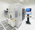
MEMS, 나노기술, 반도체 시장용 웨이퍼 본딩 및 리소그래피 장비 전문 기업인 EV Group(이하 EVG)가 새로워진 디자인의 200㎜ 레지스트 처리 장비를 선보이며, 이전 세대의 우수한 성능을 바탕으로 모듈 용량을 늘려 생산성을 높였다.
EVG는 자사의 리소그래피 솔루션 포트폴리오에 속하는 차세대 200㎜ 제품으로서 EVGⓡ150 자동화 레지스트 처리 시스템을 출시한다고 8일 밝혔다.
새로운 디자인의 EVG150 플랫폼은 이전 세대 플랫폼과 비교해서 최대 80퍼센트까지 더 높은 생산성, 우수한 범용성, 50퍼센트 더 작은 풋프린트가 특징이다.
범용 플랫폼으로서 신뢰할 수 있는 고품질 코팅 및 현상 공정을 가능하게 하므로, 첨단 패키징, MEMS, RF, 3D 센싱, 전력 반도체, 포토닉스를 비롯한 다양한 디바이스 및 애플리케이션에 적용할 수 있다. 새로운 장비는 우수한 생산성과 유연성 및 반복성을 통해 대량 생산과 산업용 개발 양쪽 모두의 까다로운 요구를 충족한다.
세계적인 EBS(electronic based system) 연구 센터인 실리콘 오스트리아 랩스(Silicon Austria Labs)는 차세대 EVG150 시스템의 첫 번째 고객이다.
실리콘 오스트리아 랩스의 마이크로시스템 연구 부문장인 모센 모리디(Mohssen Moridi) 박사는 “우리는 선도적인 제조회사들과 협력해서 인더스트리 4.0, 사물 인터넷(IoT), 자율 운전, 사이버-물리 시스템(CPS), 인공지능(AI), 스마트 시티, 스마트 에너지, 스마트 의료의 토대를 마련하는 기술들을 개발하고 있다”며 “EVG의 차세대 EVG150 레지스트 처리 시스템은 유연성이 뛰어나 EBS 혁신을 촉진하는 우리의 개발 고객들과 함께 새로운 공정과 제품의 대규모 구현을 위한 발판을 마련하는 데 도움이 된다”고 말했다.
200㎜ 기판용 차세대 EVG150은 이전 세대 플랫폼의 업계 선도적인 특성을 그대로 유지하고 있다. 이러한 특성으로는, 회전 및 분사 코팅, 현상, 베이크 및 냉각 공정을 위해 맞춤형 모듈 구성이 가능한 완벽하게 자동화된 플랫폼, 극히 복잡한 형태의 컨포멀 코팅이 가능한 EVG 고유의 OmniSprayⓡ 기술, 지속적으로 높은 생산성을 달성하도록 듀얼 엔드 이펙터 기능을 사용하는 정교하고 성능이 검증된 로봇 핸들링, 그리고 웨이퍼 에지 핸들링과 휘거나 뒤틀린 웨이퍼, 또는 박막 웨이퍼를 취급할 수 있는 능력이 포함된다.
EVG의 기업 테크놀로지 디렉터인 토마스 글린스너(Thomas Glinsner) 박사는 “레지스트와 패터닝 공정은 반도체 제조에 있어서 가장 반복적으로 사용되는 공정들이다. EVG는 리소그래피와 회전 및 분사 코팅 등의 공정 분야에서 다년간 쌓아온 전문성을 바탕으로 고객들의 극히 까다로운 요구를 충족하는 솔루션을 제공한다”며 “차세대 EVG150 시스템은 이러한 경험을 토대로 탄생한 것으로서, 범용 플랫폼으로 새로운 차원의 생산성과 비용 상의 이점을 달성하도록 설계되었으며 전례 없이 뛰어난 유연성으로 다양한 애플리케이션의 레지스트 공정 요구를 충족한다”고 말했다.

관련뉴스
-

EVG, 나노종합기술원 등과 협력하여 새로운 디스플레이 코팅 기술 개발
EV 그룹(EVG)은 학계, 연구기관, 산업체를 위한 나노기술 R&D 중심인 나노종합기술원(NNFC)과 원재료 제조 및 공정서비스를 제공하는 NNFC에서 분사한 토탈 솔루션 업체 나노 이니쉐이티브 (NI: Nano Initiative)와 공동으로, 현재 초기 결과들을 비롯해 디스플레이를 위한 개선된 투명 나노 구조화 반사-방지 코팅(nanostructured anti-reflective coating)을 생산하기 위한 공동개발프로그램 (JDP)의 제시 방향을 발표했다. 공동개발프로그램을 진행해온 3사 협력사들은, 대부분의 고분자 코팅(polymeric coatings) 보다 우수한 97 퍼센트 이상의 투과율과 표면경도 3H를 제공하는 뛰어난 구조 복제의 반사방지 코팅(nanostructured anti-reflective coating)을 성공적으로 입증했다. 이와 대조적으로, 현재 박막광학 코팅(thin-film coatings) 기술은 92 퍼센트의 투과율만 제공한다.
2016-07-13 오후 2:33:15by 김수지 기자
-
EVG, 다기능 마이크로·나노임프린트 솔루션 ‘EVG®7300’ 출시
자유도와 높은 정밀도로 나노 및 마이크로 광학 부품과 기기를 대량 생산하고자 하는 사용자의 요구를 충족할 수 있는 최첨단 솔루션이 등장했다. EV 그룹(이하 EVG)이 자동화된 SmartNIL® 나노임프린트 및 웨이퍼 레벨 광학 시스템인 EVG®7300을 출시한다.
2022-01-19 오후 12:01:08by 성유창 기자
-
EVG, ITRI에 반도체 장비 공급
MEMS, 나노기술, 반도체 시장용 웨이퍼 본딩 및 리소그래피 장비 분야를 선도하는 EV Group이 대만 ITRI에 웨이퍼 본딩 및 리소그래피 장비를 공급하며, 반도체 개발에 서로 협력한다.
2022-09-06 오후 3:16:26by 배종인 기자

.jpg)
많이 본 뉴스
[열린보도원칙] 당 매체는 독자와 취재원 등 뉴스이용자의 권리 보장을 위해 반론이나 정정보도, 추후보도를 요청할 수 있는 창구를 열어두고 있음을 알려드립니다.
고충처리인 장은성 070-4699-5321 , news@e4ds.com