[연재]ST 유지 카와노 엔지니어(21)-MCU가 사인파와 코사인파를 생성할 수 있는가?
기사입력 2022.11.14 14:00
MCU, RAM 사용 없이 삼각파 생성 가능
소프트웨어 사용 y=ax+b 생성, 일정한 사이클로 x 증가
임의 파형, RAM 데이터 테이블 준비 후 DAC 이 값 출력
[편집자주]일반적으로 반도체라 하면 컴퓨터의 CPU와 메모리처럼 일반인에게 익숙한 반도체를 떠올리기 마련이다. 반면에 전자제품 구동을 위해서 핵심 반도체로 쓰이는 MCU(Micro Controller Unit)의 경우 일반적으로 우리가 쉽게 접하는 모든 전자제품에서 사용되고 있으면서도 일반인에게는 아직 낯선 반도체다. 이런 MCU가 최근 반도체 부족 사태로 인해 언론에 오르내리며, 일반인들에게 주목받기 시작했다. 이에 본지는 MCU 반도체 전문기업인 ST마이크로일렉트로닉스의 유지 카와노 매니저의 연재기고를 통해 MCU에 대해 전문적으로 알아보는 자리를 마련했다.
 ■ 질문
■ 질문MCU가 사인파(sine wave)와 코사인파(cosine wave)를 생성할 수 있는가? 주파수도 변경이 가능한가?
■ 답변
MCU가 DAC(digital-to-analog converter)를 내장하고 있다면, MCU를 사용하여 사인파 또는 코사인파를 생성할 수 있다. DAC는 지정된 범위 내에서 임의의 아날로그 전압을 출력할 수 있다. 예를 들어, DAC가 10 bit의 해상도를 지원한다면 2에서부터 2의 거듭제곱의 범위, 즉 (1,024) 1 = 1,023 단계(step)까지 전압을 표현할 수 있으며, 출력 전압은 사용자가 레지스터에 할당한 값(1,023 이하)에 대응하게 된다. 출력 사이클을 변경하면 주파수를 바꿀 수 있다.
파형을 생성하려면, 먼저 RAM에 출력할 전압 테이블을 저장해야 한다. 그 후에는 DAC가 주기적으로 값들을 순차적으로 출력하도록 해야 한다. 사인파와 코사인파 뿐만 아니라 다른 형태의 임의 파형을 출력할 수 있는지에 대해서도 관심이 있을 것이다.
그림 1은 18 단계의 출력 사이클로 생성된 사인파의 예를 나타낸 것이다. 10bit 해상도를 지원하는 DAC는 출력 값을 최대 1,023단계까지 변경할 수 있다. 출력 단자에서 커패시터를 사용해 출력 신호를 필터링함으로써 거의 이상적인 평활도의 사인파형을 얻을 수 있다.
CPU 또는 DMA는 타이머에 의해 결정된 고정 사이클로 데이터를 RAM에서 DAC로 전송한다. 최고 전압은 1.00 V이다. 주파수의 파형을 변경하려면, 타이머 사이클을 변화시켜 출력 데이터의 스위칭 간격만 조정하면 된다.
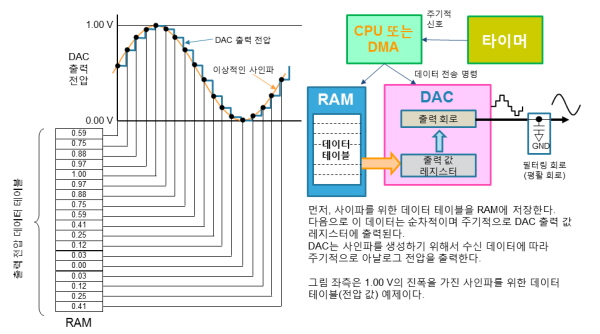
▲그림1 : DAC를 이용한 사인파 생성 방법
■ 설명
○ DAC의 동작 원리
n bit의 해상도를 지원하는 DAC는 2²-1로 기준 전압(Vref)을 나누어 얻은 단계로 출력 전압을 설정할 수 있다. 예를 들어, 10 bit의 해상도와 Vref가 1.0 V인 경우에 출력 전압을 위한 1단계를 다음 식을 통해 구할 수 있다: 1.0V÷1023(=2¹⁰-1)=0.0009775V. 이를 위해서 출력 전압 레지스터는 10bit를 제공해야 한다. 이제 출력 값 레지스터가 m의 값을 가질 경우, DAC는 m×0.0009775V의 전압을 출력한다. 결과적으로 출력 값 레지스터가 [0000000000]의 이진 값(binary value)을 가지고 있을 경우, 0×0.0009775V=0V의 전압을, 이진 값이 [1000000000]이면, 512×0.0009775V=0.5005V의 전압을, 그리고 이진 값이 [1111111111]일 경우, 1023×0.0009775V=1.0V(max)의 전압을 출력한다.
○ DAC 방식
전압을 분할하는 데 사용할 수 있는 다양한 방식이 있지만, MCU의 DAC는 Vref가 직렬로 연결된 저항들에 의해 분할되는 사다리 저항(ladder resistance) 방식을 사용하는 경향이 있다. 그림 2는 사용할 수 있는 가장 간단한 방식을 나타낸 것으로, 저항들을 직렬로 간단하게 연결하여 전압을 분할할 수 있다. 이를 직렬 저항 방식(series resistance method)이라고 하며, 전압 선택 형태로도 알려져 있다.
10bit DAC는 1,023개의 레지스터를 필요로 하며, 12 bit DAC는 4,095개의 레지스터를, 16bit DAC는 65,535개의 레지스터를 필요로 한다(그림 2는 4 bit 해상도를 지원하는 DAC를 나타낸 것이다). 그러나 원하지 않는 변동 없이 실리콘 웨이퍼 상에 이렇게 많은 레지스터를 제조하는 것은 거의 불가능하며 상당히 비현실적이다. 사실 직렬 저항 방식은 10bit 이상의 해상도를 지원하는 DAC에 사용된다. 보다 높은 해상도를 위해서는 R-2R 방식 또는 바이너리 저항 방식이 일반적으로 사용된다.
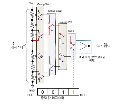
▲그림 2 : DAC 방식 (직렬 저항 방식)
이 글의 초점은 MCU의 기능이기 때문에 이해하기 쉬운 간단한 구조를 가진 직렬 저항 방식에 대해서만 살펴보기로 하자. 다른 방식에 대해서는 다음 URL(http://ednjapan.com/edn/articles/0704/01/news003.html)(일어만 지원)에서 DAC 아키텍처에 대한 글들을 참고하기 바란다.
이제, 출력 값 레지스터의 각 bit는 스위칭 그룹에 대응한다. SW1 그룹은 0 지점의 bit(LSB)와, SW2 그룹은 첫 번째 bit와, SW3 그룹은 두 번째 bit와 그리고 SW4 그룹은 세 번째 bit(MSB)와 대응한다. 각 bit가 1로 설정되면 해당 그룹의 모든 스위치는 Vref 측에 연결되고, 각 bit가 0으로 설정되면 GND 측에 연결된다.
그림 2는 출력 값 레지스터가 이진수 1100으로 설정된 경우의 DAC 방식을 나타낸 것이다. SW3 및 SW4 스위치는 Vref측에 연결되고, SW1 및 SW2 스위치는 GND 측에 연결된다. 이러한 구성에서 출력 단자 Vout은 Vref의 12/15의 전압을 가진다. 레지스터 값이 분자와 동일하기 때문에 이러한 매우 간단한 회로를 통해 출력 전압을 생성할 수 있다.
○ DAC 구동 성능 및 파형 평활도 개선 방법
일부 DAC의 경우, DAC 출력 단자를 형성하기 위해 레지스터와 스위치로부터의 출력이 MCU 단자에 직접 연결된다. 이와 같은 경우, 각기 다른 전압이 각기 다른 레지스터 조합과 일치하게 되어 각기 다른 출력 임피던스 값들이 나타나고 출력 저항으로 구동 성능은 감소하게 된다. 이러한 이유로 인해 DAC 출력 단자는 구동 성능을 강화하기 위해서 일반적으로 증폭기를 제공한다.
그림 2는 OP 앰프 전압 폴로워(follower)를 사용할 경우를 예로 나타낸 것이다. 하지만, 출력 단자에 OP 앰프와 같은 아날로그 회로를 사용하면 아날로그 이득(풀-스케일) 에러 또는 오프셋 에러가 발생할 수 있기 때문에 DAC가 0 V 및 Vref의 값을 정확하게 출력할 수 없다.
일반적으로 사용자는 MCU를 통해 신호를 직접 출력할지 또는 증폭기를 통해 출력할지를 선택할 수 있다.
DAC는 심지어 최고 해상도에서도 파형을 단계적으로 출력한다. 이상적인 평활한 아날로그 파형을 얻기 위해서 평활 회로(smoothing circuit)를 출력 단자에 설치한다. 대역-통과 필터는 이상적인 솔루션이지만, 출력과 GND를 통과하는 커패시터가 효과적일 수 있다.
○ 사이클(주파수) 제어
DAC 출력 값 레지스터를 재작성하는 주기를 변경하면 주파수를 변경할 수 있다. 그림 1은 0.0556s(1s/18)의 주기로 출력 값 레지스터를 재작성하여 1 Hz의 주파수를 가지는 사인파의 생성 과정을 나타낸 것이다.
일정한 사이클로 DAC 출력 값 레지스터를 재작성하기 위해서는 타이머와 같은 시간-측정 기능을 사용해야만 한다. 출력 값 레지스터를 실제로 재작성하는 것은 CPU이지만, MCU가 DMA(direct memory access) 성능을 제공한다면 DMA 모드에서 레지스터를 재작성할 수 있다. 이를 통해 CPU는 증가된 효율로 다른 태스크들을 수행할 수 있다.
타이머를 사용하여 CPU 또는 DMA(인터럽트 포함)를 일정한 주기로 트리거하면 RAM 테이블 데이터로 DAC 출력 값 레지스터 데이터를 대체할 수 있다. 사인파를 위한 값으로 RAM 테이블 데이터를 설정하면 DAC가 사인파를 생성할 수 있다.
동일한 파형을 반복적으로 출력하기 위해서는 RAM 테이블에 1개의 주기를 위한 데이터를 설정하여 MCU가 데이터를 반복적으로 읽게 해야 한다. RAM 테이블의 동일한 데이터를 반복적으로 사용하는 이 방식을 순환 모드(circular mode)라고 한다.
○ 정현파 이외의 파형 생성 방법
사인파를 생성하는 데 사용하는 RAM 테이블 데이터는 코사인파 생성에도 사용이 가능하다. 사인파와 코사인파 사이의 유일한 차이는 90°의 위상차이다. 코사인파를 생성하려면, MCU가 90°에 대응하는 값부터 시작하여 테이블을 읽게만 하면 된다(그림 3(a) 참조).
삼각파를 생성하기 위해서는 RAM 테이블 데이터가 일정한 기울기(gradient)에서 선형적으로 증가하도록 설정해야 한다. 최댓값에 도달할 때까지 순차적으로 MCU가 데이터를 읽도록 한 다음, 데이터를 역방향으로 읽게 해야 한다. 이러한 방법으로 균등 증가(equal increasing) 및 감소 절대(decreasing absolute) 기울기를 가지는 삼각파를 생성할 수 있다(그림 3(b) 참조). 일반적으로는 RAM에 테이블을 만드는 대신, 다음의 과정을 따르는 것이 최상의 방법이다: 소프트웨어를 사용하여 y = ax + b의 공식을 생성하고, y를 계산하기 위해 일정한 사이클로 x를 증가시킨 다음에 계산 결과를 DAC 출력 값 레지스터에 입력한다. 이를 통해 RAM을 사용하지 않고도 삼각파를 생성할 수 있다.
잡음파(noise wave)를 만들기 위해서는 난수를 생성한 다음 DAC가 그 값들을 출력하도록 해야 한다. 일부 최신 MCU는 난수 생성 기능을 지원하기 때문에 잡음파를 만드는 것이 상대적으로 간단하다.
임의 파형을 만들기 위해서는 RAM에 생성하고자 하는 파형과 일치하는 데이터 테이블을 준비한 다음에 DAC가 이 값을 출력하도록 하면 된다.
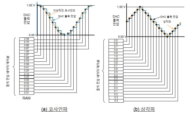
▲그림3 : DAC를 이용한 코사인파/삼각파 생성 방법
관련뉴스
-

[연재]ST 유지 카와노 엔지니어(18)-사용하지 않는 GPIO를 어떻게 처리할 수 있는가?
MCU는 CPU나 GPU와 다르게 낯설지만, 가장 많이 사용되는 반도체 중 하나다. ST 시스템 솔루션 랩의 유지 카와노 매니저에게 MCU의 활용성과 가능성이 얼마나 큰지 들어보자.
2022-06-14 오후 12:14:02by 편집부
-

[연재]ST 유지 카와노 엔지니어(19)-어떻게 MCU가 고휘도 LED를 직접 구동할 수 있게 할 수 있는가?
MCU는 CPU나 GPU와 다르게 낯설지만, 가장 많이 사용되는 반도체 중 하나다. ST 시스템 솔루션 랩의 유지 카와노 매니저에게 MCU의 활용성과 가능성이 얼마나 큰지 들어보자.
2022-07-04 오후 2:26:25by 편집부
-

[연재]ST 유지 카와노 엔지니어(20)-UART 통신은 외부 발진 소자 없이 동작이 가능한가?
MCU는 CPU나 GPU와 다르게 낯설지만, 가장 많이 사용되는 반도체 중 하나다. ST 시스템 솔루션 랩의 유지 카와노 매니저에게 MCU의 활용성과 가능성이 얼마나 큰지 들어보자.
2022-11-02 오후 2:56:07by 편집부


많이 본 뉴스
[열린보도원칙] 당 매체는 독자와 취재원 등 뉴스이용자의 권리 보장을 위해 반론이나 정정보도, 추후보도를 요청할 수 있는 창구를 열어두고 있음을 알려드립니다.
고충처리인 장은성 070-4699-5321 , news@e4ds.com