어플라이드, CFE 기술로 1나노 이하 불량도 잡는다
기사입력 2023.02.13 16:20
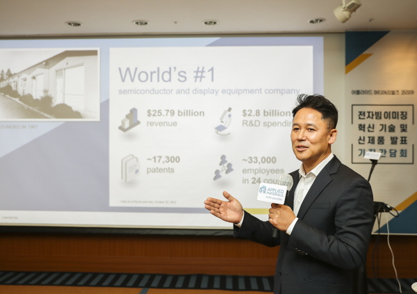
▲박광선 어플라이드 머티어리얼즈 대표이사가 회사를 소개하고 있다.
eBeam ‘SEM비전 G10’·‘프라임비전 10’ 발표
분해능 최대 50%·이미징 속도 최대 10배 향상
분해능 최대 50%·이미징 속도 최대 10배 향상
재료공학 솔루션 분야 글로벌 선도 기업 어플라이드 머티어리얼즈(Applied Materials)가 냉전계 방출(CFE) 기술 상용화로 전자빔 이미징 기술을 혁신하며, 세계 최첨단 반도체 개발을 가속화했다.
어플라이드 머티어리얼즈는 13일 기자간담회를 통해 전자빔(eBeam) 이미징의 혁신인 ‘냉전계 방출(CFE, Cold Field Emission)’ 기술을 상용화했다고 밝혔다.
또한 자사 최초 CFE 기술에 기반한 전자빔 시스템 ‘SEM비전 G10(SEMVisionⓡ G10)’, ‘프라임비전 10(PrimeVisionⓡ 10)’ 2종을 출시했다.
CFE 기술을 통해 고객들은 나노미터 단위의 기저부 결함에 대한 검사 및 이미징 작업을 향상시킬 수 있다.
기존 광학 시스템은 빠른 속도가 장점으로 웨이퍼 전체를 살펴볼 수 있지만 100㎚ 이하는 자세한 측정이 불가능했다.
이에 초미세 반도체 결함 확인을 위해 반도체 제조사들은 전자빔(eBeam) 장비를 사용해왔다.
전자빔 장비는 웨이퍼 전체는 불가능하지만 1.2㎚까지 계측 검사가 가능해 초미세 반도체 검사에 있어서 필수적으로 사용돼 왔다.
하지만 기존 고온전계 방출형(TFE, Thermal Field Emission) 전자빔 시스템은 섭씨 1,500℃ 이상에서 작동해 온도를 낮추면 빔 폭은 좁아지고 전자 개수가 많아지는 문제가 있었다.
반면에 이번에 어플라이드가 새로 출시한 CFE 기술을 가진 전자빔은 26℃에서 작동하고, 1㎚ 이하의 이미지 분해능 및 10배 빠른 이미징 속도를 구현 할 수 있다.
이 기술의 상용화로 차세대 GAA(Gate-All-Around) 로직 칩은 물론 고집적도 D램, 3D 낸드 메모리 개발 및 생산 속도가 크게 빨라질 전망이다.
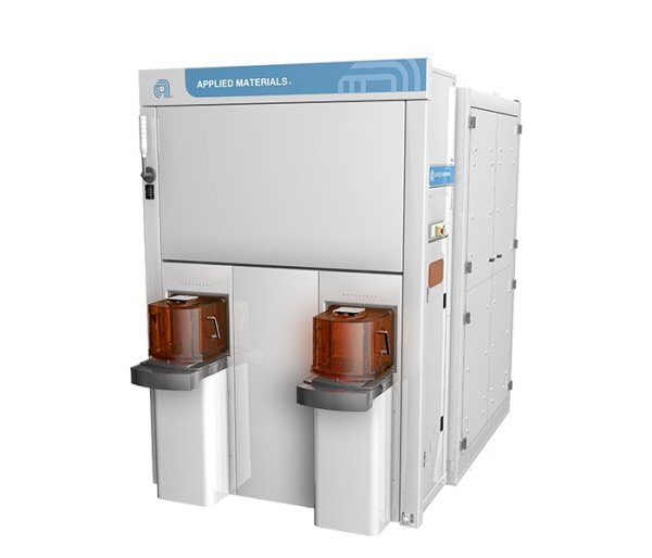
▲어플라이드 머티어리얼즈 ‘SEM비전 G10’ 시스템
모든 로직 GAA 고객사가 SEM비전 G10 시스템을 공정 개발 툴로 선택해 이 시스템은 이미 4억달러 이상의 매출을 거뒀다.
또한 유수의 메모리 고객사들이 신규 D램과 낸드 공정 노드를 개발하고 기존 메모리 노드의 대량 생산 능력 확대를 위해 SEM비전 G10 시스템을 배치하고 있다.
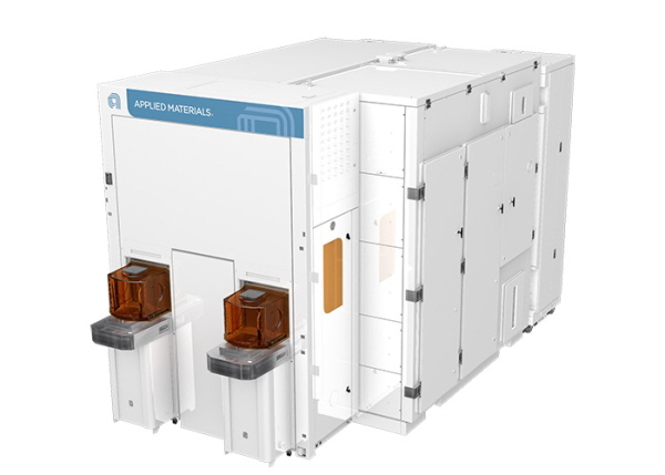
▲어플라이드 머티어리얼즈 ‘프라임비전 10’ 시스템
프라임비전 10 결함 검출 시스템은 어플라이드 전자빔 포트폴리오에 새롭게 합류된 제품이다.
이 시스템은 웨이퍼 표면 미세 결함을 검사하기 위한 나노미터 단위의 분해능은 물론 3D GAA 구조 로직 소자 및 고종횡비(High Aspect Ratio) 메모리 소자의 수율에 영향을 미치는 치명적 결함을 검사하는 3D 검사 기술을 특징으로 한다.
프라임비전 10 시스템은 높은 전자빔 밀도로 TFE 기반 전자빔 계측 시스템보다 최대 10배 빠른 속도로 고분해능 이미지를 생성할 수 있다.
한편 어플라이드 머티어리얼즈는 2021년도에 10억달러 이상의 수익과 50%가 넘는 전자빔 시장 점유율 기록하며 공정 제어 업계에서 전자빔 시스템 분야 최대 공급 업체로 떠올랐다.

관련뉴스
-

어플라이드 머티어리얼즈 코리아, 박광선 신임 사장 선임
재료공학 솔루션 분야 글로벌 선도 기업 어플라이드 머티어리얼즈 코리아의 신임 박광선 사장이 취임했다.
2022-11-03 오전 8:43:01by 배종인 기자
-

어플라이드, 2022년 매출 257억9천만불…전년比 12% ↑
어플라이드 머티어리얼즈가 2022년 글로벌 반도체 시장 호황에 힘입어 영업이익률 30.2%를 달성하는 기록적인 실적을 거뒀다.
2022-11-18 오후 3:27:29by 배종인 기자
-

[세미콘 코리아 2023]어플라이드, 반도체 기술 변곡점 혁신 솔루션 제시
재료공학 솔루션 분야 글로벌 선도 기업 어플라이드 머티어리얼즈 코리아(대표 박광선)가 세미콘코리아 2023에서 반도체 기술 변곡점에 대한 혁신 솔루션을 제시한다.
2023-01-30 오후 4:30:55by 배종인 기자

.jpg)
많이 본 뉴스

[열린보도원칙] 당 매체는 독자와 취재원 등 뉴스이용자의 권리 보장을 위해 반론이나 정정보도, 추후보도를 요청할 수 있는 창구를 열어두고 있음을 알려드립니다.
고충처리인 장은성 070-4699-5321 , news@e4ds.com