어플라이드, EUV 노광 공정 수 획기적으로 줄인다
기사입력 2023.03.02 09:28
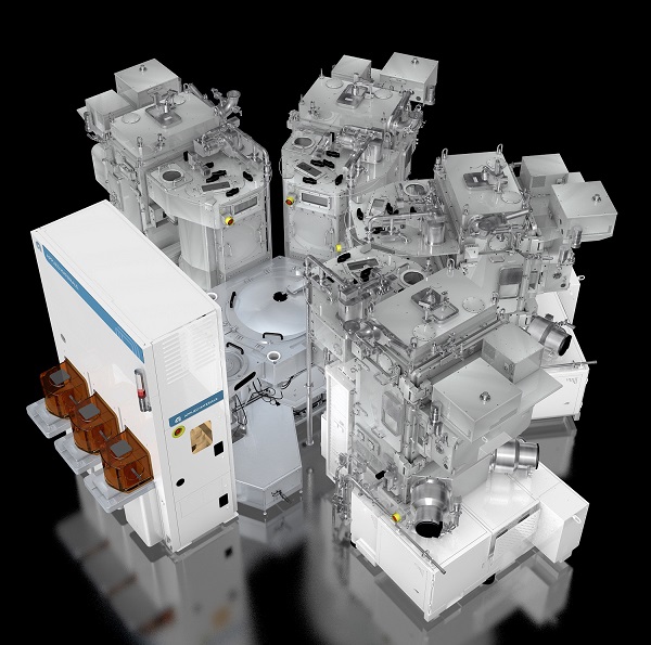
Centura Sculpta 패터닝, 빠르고·간소·비용 효과적
기존 EUV 더블 패터닝 시스템 대비 빠르고 간소하며 비용 효과적인 새로운 패터닝 시스템이 등장해 첨단 반도체 제조에 있어 노광 공정을 줄일 수 있는 혁신적 대안으로 떠오르고 있다.
어플라이드 머티어리얼즈는 2일 ‘Centura Sculpta’ 패터닝 시스템을 공개했다.
이 기술을 통해 반도체 제조사는 고성능 트랜지스터 제작 및 배선층 제작 과정에서 EUV 노광 스텝(step)을 줄임으로써 첨단 반도체 제조에 소요되는 비용 및 복잡성을 낮추면서, 환경에 미치는 영향을 줄일 수 있다.
고객들은 EUV의 분해능(resolution) 한계보다 작은 반도체 소자를 프린팅할 때 칩 면적 최적화를 위해 EUV 더블 패터닝 사용을 확대하고 있다.
반도체 제조사는 고밀도 패턴을 절반으로 분할하여 프린팅하는 EUV 더블 패터닝을 사용해 EUV의 분해능 한계에 대응하는데 이때 마스크 2개가 제작되고 절반으로 분할된 패턴은 모두 층간 패터닝 필름에 결합된 후 웨이퍼에 식각된다.
이러한 더블 패터닝은 소자 밀도 증대 측면에서 효과적이지만 설계와 패터닝을 복잡하게 하고 시간, 에너지, 재료, 물이 소비되는 여러 공정 스텝이 필요해 웨이퍼 팹 및 웨이퍼 생산 비용을 높인다.
어플라이드 머티어리얼즈는 추가적인 비용, 복잡성, 에너지, 재료 소비 없이 반도체 제조사가 설계를 축소할 수 있도록 여러 주요 고객사와 긴밀히 협력해 ‘Centrua Sculpta’ 패터닝 시스템을 개발했다.
반도체 제조사는 싱글 EUV 패턴을 프린팅한 다음 Sculpta 시스템을 사용해 패턴 형태를 원하는 방향으로 길게 늘려 소자 간 간격을 줄이고 패턴 밀도를 높일 수 있다. 최종 패턴은 싱글 마스크로부터 생성되기 때문에 설계비용과 복잡성이 줄어들고 더블 패터닝 정렬 오류로 인한 수율 저하 위험도 사라진다.
EUV 더블 패터닝에는 CVD(화학기상증착) 패터닝 필름 증착, CMP(화학기계연마) 세정, 포토레지스트 증착 및 제거, EUV 노광, 전자빔 계측, 패터닝 필름 식각, 웨이퍼 세정 등 여러 단계의 추가 제조 공정 스텝이 요구된다.
Sculpta 시스템은 EUV 더블 패터닝의 각 시퀀스를 대체하며 반도체 제조사에게 △10만 WSPM(Wafer Starts Per Month) 생산능력당 2억5,000만 달러 이상의 자본 비용 절감 △웨이퍼당 50달러 이상의 생산 비용 절감 △웨이퍼당 15kWh 이상의 에너지 절감 △웨이퍼당 0.35kg 이상의 이산화탄소에 해당하는 직접 온실가스 배출량 감축 △웨이퍼당 15리터 이상의 용수 절감 등의 혜택을 제공한다.
프라부 라자(Prabu Raja) 어플라이드 머티어리얼즈 반도체 사업부 수석 부사장 겸 총괄 매니저는 “새로운 Sculpta 시스템은 재료 공학 발전이 EUV 노광을 보완함으로써 반도체 제조사가 칩 면적 및 비용을 최적화함과 동시에 첨단 반도체 생산 분야에서 증가하는 경제·환경 문제를 해결하는데 어떤 역할을 할 수 있는지 보여주는 좋은 사례”라며 “Sculpta 시스템 특유의 패터닝 형성 기술은 어플라이드의 리본 빔(ribbon-beam)과 재료 식각 기술을 결합, 패터닝 엔지니어의 툴킷을 위한 획기적 혁신”이라고 밝혔다.




많이 본 뉴스

[열린보도원칙] 당 매체는 독자와 취재원 등 뉴스이용자의 권리 보장을 위해 반론이나 정정보도, 추후보도를 요청할 수 있는 창구를 열어두고 있음을 알려드립니다.
고충처리인 장은성 070-4699-5321 , news@e4ds.com