상용화 단계 접어든 차세대 3종 메모리 'MRAM, PCRAM, ReRAM'의 특징과 전망
기사입력 2019.06.13 10:27
| MRAM, AIoT 기기 주요 메모리 후보
| PCRAM, DRAM 기반 DIMM, SSD 대체
| ReRAM, 스토리지 애플리케이션에서 가치
MRAM(Magnetic RAM; 자성메모리), PCRAM(Phase Change RAM; 상변화메모리), ReRAM(Resistive RAM; 저항메모리) 3종의 새로운 메모리가 수십 년 연구 끝에 상용화 단계로 접어들면서 반도체와 컴퓨팅 산업에 호재가 되고 있다. 이 3가지 메모리를 생산하기 위해서는 새로운 소재가 필요하며, 공정 기술 및 제조 분야 혁신을 필요로 한다.
차세대 3종 메모리 MRAM, PCRAM, ReRAM의 특징과 전망
이상적인 반도체 메모리는 ▲빠른 읽기 속도 ▲빠른 쓰기 속도 ▲랜덤 액세스 ▲저비용 ▲3D 확장성 ▲저전력 ▲비휘발성 ▲높은 내구성 ▲높은 온도 허용오차 ▲멀티 비트 저장을 위한 멀티 스테이트(multiple states)와 같은 특징들을 모두 제공해야 한다. 현재 어떤 메모리도 이를 모두 제공하지 않는다.
MRAM, PCRAM, ReRAM과 같은 신종 메모리는 주류 메모리를 보완할 주요 후보다. 성능 개선, 전력 및 비용 절감을 보장하고 주류 메모리를 대신할 이 차세대 메모리 3종의 특징을 살펴보자.
MRAM, IoT 기기의 주요 메모리 후보
MRAM은 빠른 속도, 비휘발성, 저전력(마그네틱 기술)뿐만 아니라 메모리 배열이 단 3개의 부가 마스크(additional masks)로 백엔드 인터커넥트 레이어에 내장될 수 있어 경제성이 높다.
MRAM은 SRAM보다 느리지만 많은 내장 컴퓨팅 애플리케이션의 작업 메모리로 사용될 수 있을 만큼 빠르다. 또한 레벨3 캐시 요구를 충족할 정도로 빠르다.
여러 로직∙파운드리 선도 기업은 내장 MRAM을 사용한 SoC 설계의 조기 생산을 발표했다.
MRAM은 특히 AI 연산을 지원해야 할 IoT 기기의 주요 메모리 후보가 되고 있다. 시간이 지날수록 MRAM은 임베디드 시장의 자동차 분야에서 고온 요구 조건을 충족시킬 수 있을 것이다.
기술 및 제조 관점에서 MRAM의 가장 큰 과제는 디지털 데이터를 나타내는 데 기본 프로그래밍 요소인 MTJ(Magnetic Tunnel Junction) 형성에 필요한 많은 박막 스택을 정확히 증착하는 것이다. 많은 금속 및 절연층은 대기보다 낮고 깨끗한 고진공 상태에서 PVD(Physical Vapor Deposition) 방법을 이용해 증착되어야 한다.
코어 산화마그네슘(MgO) 박막층은 엄격히 통제된 상태에서 정확한 결정 배열로 증착되어야 한다. 단 하나의 원자에서 높이 변화가 발생해도 성능과 신뢰성에 영향을 미칠 수 있다.
PCRAM, 새로운 스토리지 클래스 메모리
PCRAM은 프로그래밍 메커니즘으로 열에 의해 고도의 비결정 소재 배열에서 결정 배열로 전환되는 ‘상변화(phase change)’ 소재를 기반으로 한다.
PCRAM은 랜덤 액세스, DRAM보다 낮은 비용, 3D 확장성 및 비휘발성 등의 특징을 갖는다. 그 결과 주요 메모리 업체들은 PCRAM이 일부 DRAM 기반의 DIMM(Dual In-line Memory Module)과 고가의 SSD(Solid State Drive)를 대체하기 위해 비휘발성 DIMM과 같은 애플리케이션에 적합한지 평가하고 있다.
PCRAM은 임계 구조를 형성하기 위해 멀티 레이어 소재가 정확히 증착되어야 한다. PCRAM 층은 MRAM만큼 얇지 않지만 불순물에 매우 민감하다. 때문에 다양한 소재를 사용할 수 있고 미세 입자와 불순물을 예방할 수 있는 PVD 공정 기술이 요구된다. 일단 PCRAM 스택이 형성되면 플라스마 식각 방식을 이용해 개별 메모리 셀이 형성되고 캡슐화는 노출된 상변화 소재를 보호한다.
확장성은 PCRAM 비용 로드맵 추진의 핵심이다. 2D 스케일링은 CD(Critical Dimension)를 20nm 하프 피치로 줄이기 위해 사용되고 15-16nm 디자인 룰이 곧 등장할 것으로 보인다. PCRAM의 3D 스케일링은 더욱 장래성이 있다. 초기 디자인은 2레이어 스택을 이용했지만 기술 로드맵에 따르면 4레이어, 심지어 8레이어 스택도 가능할 전망이다.
ReRAM, 고밀도 애플리케이션 겨냥
ReRAM 기술은 여러 형태가 있다. 이온 브리지 내 금속 필라민트에 삽입된 ReRAM이 있는가 하면 기본 소재 내 생성된 산소 정공으로 생성되는 ReRAM도 있다. 정보 비트(bit)는 저항성 소재 중 주로 금속 산화물에 저장된다. 저항성 소재에 전류를 가해 프로그래밍이 수행되고, 각기 다른 수준의 저항성을 감지해 읽기를 수행한다. 또한 ReRAM은 광범위한 소재를 사용할 수 있다.
지금까지 ReRAM은 내구성에 한계를 보였기 때문에 소재와 제조 기술을 개선해 신뢰성을 확보할 수 있도록 실패 원인을 파악하는 노력이 필요하다. 이 문제가 해결된다면 ReRAM은 스토리지 애플리케이션에 높은 밀도와 낮은 비용을 제공할 수 있을 것이다.
오늘날 주류 메모리인 DRAM, 플래시 및 SRAM은 수십 년을 거쳐 성숙했고 지속적으로 진화하고 있다. 하지만 이 메모리는 무엇보다 성능, 전력, 비용 측면에서 스케일링이 더욱 어려워지고 있다.
컴퓨팅은 지속적으로 확장하고 있다. 많은 사람이 수백억 개의 저가 컴퓨터가 모든 산업∙소비자 제품에 내장되어 IoT를 형성하고, 퍼블릭∙프라이빗 클라우드 데이터센터에 저장되는 데이터가 폭발적으로 증가하는 세상을 상상한다.
새로운 메모리 기술은 오염되지 않은 깨끗한 환경에서 정확한 박막 증착, 측정, 식각∙제거, 캡슐화를 이용해 생성되는 구조와 새로운 소재를 이용할 것이다. 이 같은 차세대 메모리를 가공하는데 소수의 원자 변화도 매우 큰 차이를 가져온다.
이수민 기자
관련뉴스
-
급증하는 '5G 시대' IDC 트래픽… 대비책은 FPGA
최근 데이터센터의 중요성과 IoT 디바이스의 사용률이 크게 증가하고 있다. 따라서 기존 프로세서를 주로 이용하던 각종 애플리케이션 분야에서 FPGA의 수요가 점차 증가하고 있다. 특수목적으론 FPGA가 전통적인 프로세서보다 효율이 좋기 때문이다. 인텔이 알테라를 인수하고 내놓은 첫 FPGA인 애질렉스(Agilex)는 인텔의 10nm 공정으로 제작된 반도체라는 점에서 눈길을 끈다. 더욱 흥미로운 부분은 최근 공개된 차세대 인터페이스인 CXL 규격과 PCIe 5.0을 지원한다는 점이다. 애질렉스는 CPU와 GPU 같은 전용 가속기와 함께 사용해도 충분한 대역폭을 확보할 수 있다. 또, DDR5나 HBM2 같은 초고속 메모리를 지원하는데 그치지 않고 인텔 옵테인 DC 퍼시스턴트 메모리까지도 지원한다.
2019-06-03 오후 5:49:04by 이수민 기자
-
차세대 메모리 반도체 MRAM의 속도와 용량 획기적으로 늘릴 가능성 발견
서강대학교 정명화 교수 연구팀은 자성물질 사이에 숨겨진 자기적 상호작용을 규명함으로써 차세대 메모리 반도체인 자성 메모리(MRAM)의 속도와 저장용량을 한 단계 더 발전시켜줄 가능성을 입증했다. 전류를 기반으로 하는 기존 메모리와 달리, MRAM은 전자의 스핀에 의한 자성을 이용한다. 두 개의 자성물질에서 자화 방향이 같거나 반대일 때 0 또는 1의 정보가 기록된다. 많은 장점에도 불구하고 자화 방향을 바꿀 때 필요한 소비 전력이 크다는 한계가 있다. 연구팀은 자성물질에서 대칭적 상호작용에 의한 두 가지 자화 방향(동일/반대 방향)뿐 아니라 비대칭적 상호작용에 의한 자화 방향도 있음을 발견했다. 3차원 스핀 구조에 정보를 저장함으로써 MRAM의 속도와 용량을 크게 개선할 수 있게 되었다.
2019-06-10 오후 5:28:35by 이수민 기자
-
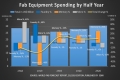
전 세계 팹 장비 투자액, 올해 줄지만 내년엔 늘어
SEMI의 최신 세계 팹 전망 보고서에 따르면, 2019년의 전 세계 팹 장비 투자액은 전년대비 19% 하락하여 484억 달러로 예상되며 2020년은 약 20% 상승하여 584억 달러에 달할 것으로 보인다. 올해 초에 SEMI가 발표한 2019년 팹 장비 투자액 성장률 전망은 -14%에서 -19%로 조정되었으며, 2020년 전망은 27%에서 20%로 하향 조정되었다. 2020년 전 세계 팹 장비 투자액은 20%의 높은 성장세에도 불구하고, 2018년 투자액 대비 약 20 억 달러 정도를 밑돌 것으로 보인다. 메모리 분야는 2019년 전체 팹 장비 투자액 감소량의 45% 가량을 차지하여 전반적인 투자액 하락의 주요 요인이 될 것으로 보인다.
2019-06-12 오전 9:16:15by 이수민 기자

많이 본 뉴스
[열린보도원칙] 당 매체는 독자와 취재원 등 뉴스이용자의 권리 보장을 위해 반론이나 정정보도, 추후보도를 요청할 수 있는 창구를 열어두고 있음을 알려드립니다.
고충처리인 장은성 070-4699-5321 , news@e4ds.com