
기사입력 2019.06.26 10:04
서강대학교 정명화 교수 연구팀은 자성물질 사이에 숨겨진 자기적 상호작용을 규명함으로써 차세대 메모리 반도체인 자성 메모리(MRAM)의 속도와 저장용량을 한 단계 더 발전시켜줄 가능성을 입증했다. 전류를 기반으로 하는 기존 메모리와 달리, MRAM은 전자의 스핀에 의한 자성을 이용한다. 두 개의 자성물질에서 자화 방향이 같거나 반대일 때 0 또는 1의 정보가 기록된다. 많은 장점에도 불구하고 자화 방향을 바꿀 때 필요한 소비 전력이 크다는 한계가 있다. 연구팀은 자성물질에서 대칭적 상호작용에 의한 두 가지 자화 방향(동일/반대 방향)뿐 아니라 비대칭적 상호작용에 의한 자화 방향도 있음을 발견했다. 3차원 스핀 구조에 정보를 저장함으로써 MRAM의 속도와 용량을 크게 개선할 수 있게 되었다.
2019-06-10 오후 5:28:35by 이수민 기자
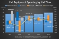
SEMI의 최신 세계 팹 전망 보고서에 따르면, 2019년의 전 세계 팹 장비 투자액은 전년대비 19% 하락하여 484억 달러로 예상되며 2020년은 약 20% 상승하여 584억 달러에 달할 것으로 보인다. 올해 초에 SEMI가 발표한 2019년 팹 장비 투자액 성장률 전망은 -14%에서 -19%로 조정되었으며, 2020년 전망은 27%에서 20%로 하향 조정되었다. 2020년 전 세계 팹 장비 투자액은 20%의 높은 성장세에도 불구하고, 2018년 투자액 대비 약 20 억 달러 정도를 밑돌 것으로 보인다. 메모리 분야는 2019년 전체 팹 장비 투자액 감소량의 45% 가량을 차지하여 전반적인 투자액 하락의 주요 요인이 될 것으로 보인다.
2019-06-12 오전 9:16:15by 이수민 기자

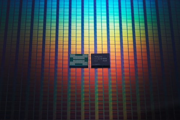
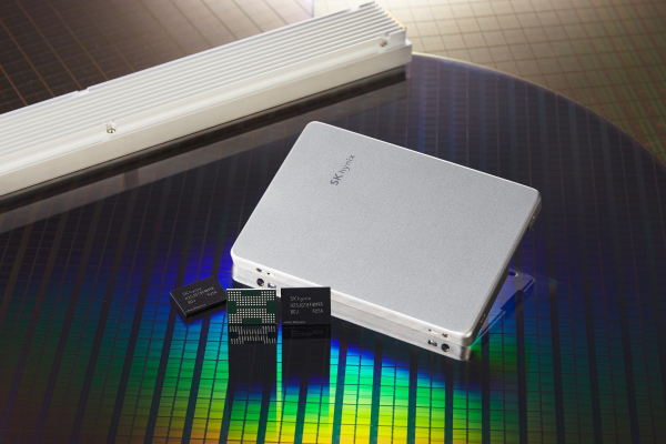
MRAM, PCRAM, ReRAM 3종의 새로운 메모리가 수십 년 연구 끝에 상용화 단계로 접어들면서 반도체와 컴퓨팅 산업에 호재가 되고 있다. 이 3가지 메모리를 생산하기 위해서는 새로운 소재가 필요하며, 공정 기술 및 제조 분야 혁신을 필요로 한다. 이상적인 반도체 메모리는 빠른 읽기 속도, 빠른 쓰기 속도, 랜덤 액세스, 저비용, 3D 확장성, 저전력, 비휘발성, 높은 내구성, 높은 온도 허용오차, 멀티 비트 저장을 위한 멀티 스테이트와 같은 특징들을 모두 제공해야 한다. 현재 어떤 메모리도 이를 모두 제공하지 않는다. 그리고 MRAM, PCRAM, ReRAM과 같은 신종 메모리는 이를 보완할 주요 후보다.
2019-06-13 오전 10:27:41by 이수민 기자


[열린보도원칙] 당 매체는 독자와 취재원 등 뉴스이용자의 권리 보장을 위해 반론이나 정정보도, 추후보도를 요청할 수 있는 창구를 열어두고 있음을 알려드립니다.
고충처리인 장은성 070-4699-5321 , news@e4ds.com