MCU는 CPU나 GPU와 다르게 낯설지만, 가장 많이 사용되는 반도체 중 하나다. ST 시스템 솔루션 랩의 유지 카와노 매니저에게 MCU의 활용성과 가능성이 얼마나 큰지 들어보자.
다양한 연산작업 ALU, MCU ‘핵심부’
모든 실제적 산술·논리연산 수행가능
복수비트 덧셈 수행 전가산기 갖춰야
[편집자주]일반적으로 반도체라 하면 컴퓨터의 CPU와 메모리처럼 일반인에게 익숙한 반도체를 떠올리기 마련이다. 반면에 전자제품 구동을 위해서 핵심 반도체로 쓰이는 MCU(Micro Controller Unit)의 경우 일반적으로 우리가 쉽게 접하는 모든 전자제품에서 사용되고 있으면서도 일반인에게는 아직 낯선 반도체다. 이런 MCU가 최근 반도체 부족 사태로 인해 언론에 오르내리며, 일반인들에게 주목받기 시작했다. 이에 본지는 MCU 반도체 전문기업인 ST마이크로일렉트로닉스의 유지 카와노 매니저의 연재기고를 통해 MCU에 대해 전문적으로 알아보는 자리를 마련했다.
 ■ ALU, MCU 핵심부
CPU(MCU의 핵심 구성요소) 안의 산술논리 연산장치(ALU, arithmetic and logic unit)는 다양한 연산 작업을 수행한다. ALU야말로 MCU의 핵심부라고 하는 것이 가장 정확한 표현일 것이다. 모든 실제적인 산술 및 논리 연산을 수행하는 부분이기 때문이다. 이제 ALU 안에서는 무슨 일이 일어나고 있는 지 살펴보자.
■ 벤 다이어그램 대신 진리표 이용 표시
ALU 안에 무엇이 들어있는지 알아내는 가장 좋은 방법은 직접 만들어 보는 것이다. 그러기 위해 먼저 가산기(adder)를 만든 뒤 간단한 논리 회로를 설계하도록 하겠다. 본고에서는 논리 연산 OR, AND 및 NOT(반전)는 물론 덧셈과 뺄셈의 산술 연산도 수행할 수 있는 ALU의 작성 방법을 살펴볼 것이다.
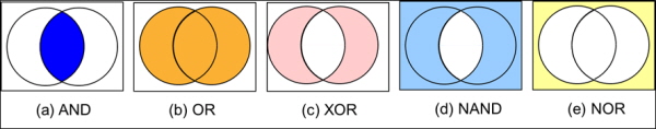
▲그림 1 : 벤 다이어그램으로 나타낸 논리 연산
ALU의 작성으로 들어가기 전에 AND, OR 및 XOR과 같은 논리 연산에 대해 잠깐 살펴보도록 하겠다. 학창 시절로 돌아가서 그 때 배웠던 벤 다이어그램을 떠올려 보자. 벤 다이어그램은 일반적으로 집합의 연구에 사용되지만, 논리 연산에도 사용될 수 있다. 이 다이어그램이 논리 연산 이해에 유용한 이유는 시각적인 도움을 제공하기 때문이다. 벤 다이어그램의 두 원형 영역들은 논리 연산의 입력 값들을 나타내며, 음영이 있는 영역들은 출력 값들을 나타낸다. 예를 들어, AND의 출력은 두 원이 겹치는 영역이며, OR의 출력은 두 원과 두 원이 겹치는 부분의 내부 영역이고, 배타적 논리합(XOR)의 출력은 양쪽 원의 내부에서 두 원이 겹치는 부분을 제외한 영역이다. MCU의 CMOS 회로에 사용되는 두 가지 연산은 NAND(AND의 논리적 보수)와 NOR(OR의 논리적 보수)이다. 그림 1은 이 다섯 가지 연산 모두에 대한 벤 다이어그램이다. MCU에서 수행되는 논리 연산에서 1은 참을, 0은 거짓을 나타낸다. 이러한 연산의 결과는 벤 다이어그램 대신에 진리표를 이용해 표시한다. AND 연산은 양쪽 입력이 모두 1일 경우에 1을 출력하며, OR 연산은 최소한 한 쪽의 입력이 1일 경우 1을 출력하며, XOR 연산은 한쪽의 입력은 1이지만 다른 쪽은 그렇지 않을 경우 1을 출력한다. 표 1은 이러한 결과들을 진리표로 요약한 것이다.
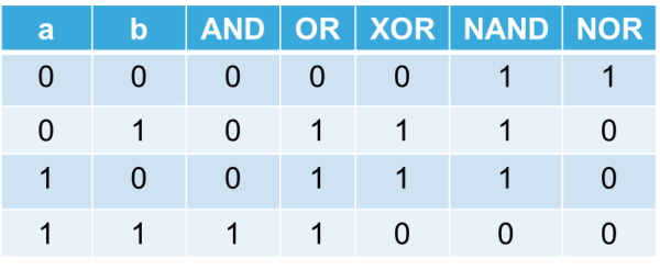
▲표 1 : 진리표, 진리표(truth table)는 다양한 논리식의 모든 입력 변수와 가능한 출력 결과들을 표 형식으로 요약한 것이다.
자, 그러면 덧셈에 대해 살펴보자. 진리표(표 1)의 XOR 열에서 볼 수 있듯이, 덧셈의 논리 연산은 XOR 연산으로 얻게 되는 것과 동일한 결과들을 제공한다. 입력 중 하나만이 1일 경우, 연산 결과도 1이 된다. 그렇지 않을 경우, 연산 결과는 0이 된다. 그러나 실제로 덧셈을 수행할 때는 다음 자리수로 넘어가는 것(자리올림)을 고려해야만 한다. 자리올림 기능과 함께 덧셈을 수행할 수 있는 회로를 가산기(adder)라고 한다. 전가산기(full adder)는 자리올림수 출력 뿐만 아니라 하위로부터의 자리올림수 입력 기능도 갖는다. 반면에 반가산기(half adder)는 이 같은 입력 기능을 갖지 않는다. 따라서 자리올림이 일어날 경우 전가산기는 자리올림 기능을 이용해 덧셈 연산을 수행하는 반면, 반가산기는 자리올림수 입력을 수용할 수 없기 때문에 자리올림수를 더하지 않는다. ALU는 복수비트 덧셈을 수행하기 때문에 전가산기를 갖춰야 한다. 이 전가산기는 하위 자리로부터의 자리올림과 함께 덧셈 연산을 수행한다.
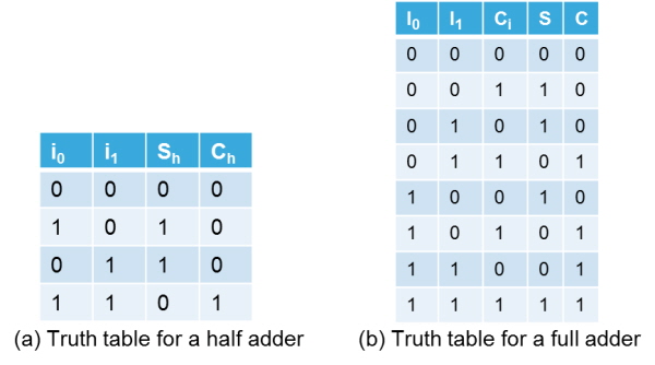
▲표 2 : 가산기 진리표
표 2(a)는 반가산기의 진리표를, 표 2(b)는 전가산기의 진리표를 보여주고 있다. 그 다음에는 이 표에 따라 논리 회로를 작성하는 방법을 살펴보자. XOR을 합계(S 또는 Sh)에, AND를 자리올림(C 또는 Ch)에 사용할 수 있다면 일이 쉬워질 것이다. 그러나 CMOS 회로의 구조 때문에 MCU의 내부 로직을 위한 AND 및 OR 회로를 작성할 수가 없다. 그 대신에 논리를 반전시키는 NAND, NOR 및 INV와 같은 회로들을 이용해야만 한다. 이 같은 회로들의 예를 그림 2(a) 및 (b)에서 볼 수 있다.
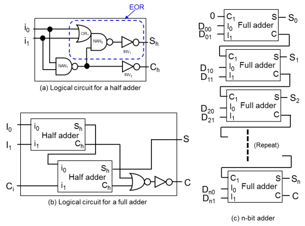
▲그림 2: 가산기
복수비트 가산기는 그림 2(c)에서 보듯이 전가산기들을 연결시킴으로써 작성할 수 있다. 예를 들어 8비트 ALU의 경우에는 8개의 전가산기를 연결시키며, 16비트 ALU의 경우에는 16개의 전가산기를 연결시키게 된다. 그러나 최하위 비트에는 하위 자리로부터의 자리올림이 수반되지 않으므로 여기에는 전가산기 대신에 반가산기를 사용할 수 있다. 실제로는 복수비트 가산기의 첫 단계에 대해서는 반가산기들을 사용할 때가 많은 것 같다.
■ 실제 MCU, 증분기 인버터 부착 뺄셈 연산 한 단계 만에 수행
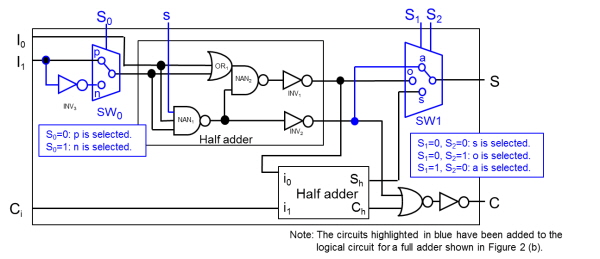
▲그림 3 : ALU 논리 회로
MCU는 2의 보수를 이용하여 간접적으로 뺄셈을 수행한다. 가산기를 이미 작성해 놓았으므로 여기에 2의 보수 회로를 추가함으로써 감산기(subtractor)를 만들 수 있다. 각각의 자리를 반전하고 끝에 1을 더해줌으로써 이진수의 2의 보수를 생성할 수 있다. 이를 위해서 방금 전 작성한 가산기의 입력 신호 중 하나에 인버터를 추가한 뒤 이어서 스위칭 회로 스위치를 붙일 수 있다. 그 모양에 대해서는 그림 3을 참조하기 바란다. 이 회로에서 그림 2(b)에서 본 것과 같은 전가산기를 위해 SW0, SW1 그리고 신호선 S0-S2와 s가 논리 회로에 추가되었다. 지금부터는 이 추가 회로들 각각에 대해 하나씩 설명하고자 한다.
먼저 SW0를 살펴보자. SW0가 p에 연결될 경우 I1은 가산기에 ‘있는 그대로’ 입력되지만, SW0가 n에 연결되면 I1은 반전된다. 이런 식으로 모든 자리들이 반전된다. 2의 보수는 I1을 반전시키고 I0에 1을 입력한 뒤 이 두 값을 더해줌으로써 얻을 수 있다. 이 숫자를 레지스터에 저장하고 이어지는 계산에서 이 2의 보수를 더해줌으로써 뺄셈을 수행할 수 있다.
실제 MCU의 ALU에서는 1을 더해주는 회로(증분기라고 한다)가 인버터에 부착되어 있어 뺄셈 연산을 한 단계 만에 수행할 수 있다.
본고의 목적은 ALU의 원리만을 살펴보는 것이므로, 여기서는 설명을 간단히 하기 위해 증분기가 없는 회로를 사용했다.
■ AND 회로
그 다음에는 몇 가지 논리 연산을 수행해 보자. 그림 2(a)를 자세히 살펴보기 바란다. AND와 OR이 둘 다 그 안에 숨어 있음을 알 수 있는가? NAN1과 INV2를 조합하면 AND가 되며, OR1과 NAN2 그리고 INV1을 조합하면 OR이 된다.
그러나 이러한 연산 기능 중 어느 쪽도 아직은 사용할 수 없다. 먼저 여기서 AND와 OR을 꺼내야만 한다. 이를 위해서 위에서 언급한 바 있는 그림 3의 추가 회로들을 이용할 것이다.
계속 진행하기 전에, (C)를 자리올림 하는 대신에 NAN1과 INV2의 결과를 S로 출력하게 되면 I0와 I1에 대한 AND 연산이 수행된다는 점에 유의해야 한다. 따라서 우리는 SW1을 이용할 것이다. AND 연산 기능이 필요할 경우에는 SW1을 a로 전환한다. 그렇게 되면 S는 I0와 I1의 AND 연산값이 되는데, 이것은 NAND1과 INV2로 구성된다. 여기서 우리는 s를 1로 설정한다. 이 경우, s는 NAND1의 출력값에 영향을 미치지 않으며, OR을 작성하기 위해 사용된다.
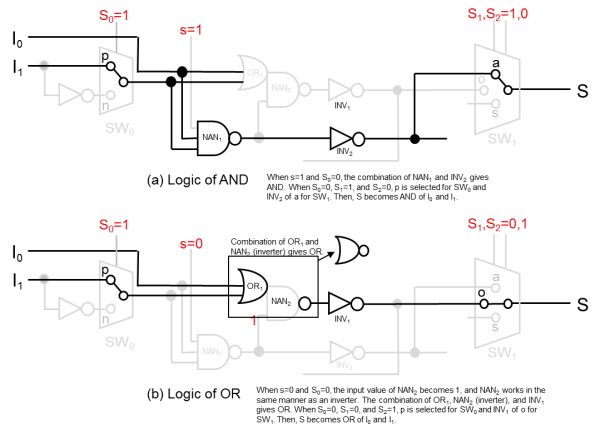
▲그림 4 : ALU AND 및 OR 회로
이 번에는 그림 4(a)를 살펴보자. 이를 좀더 쉽게 이해할 수 있도록 AND 회로를 구성하는 요소들만을 진하게 표시해 강조했다.
이제 AND 회로에 대해 좀더 잘 알게 되었으므로 그림 3으로 돌아가서 OR 회로에 대해 생각해 보자.
■ OR 회로
이번에는 OR1과 NAN2 그리고 INV1을 조합하면 OR이 되며, 여기서 신호 s를 사용한다. s=0로 설정하면 NAN1의 출력은 1로 고정된다. 이것은 NAN2의 입력값이므로(즉, NAN2의 입력값은 1로 고정된다), NAN2는 인버터와 동일한 방식으로 동작하게 된다. 그 결과, NAN2는 인버터가 되므로, OR1과 NAN2를 합성한 게이트는 NOR이 된다.
이 NOR과 INV1을 조합하면 OR이 된다. 최종적으로, SW1을 o로 전환하면 S는 I1과 I0를 OR 연산한 결과가 된다.
이 번에는 그림 4(b)를 살펴보자. 이를 좀더 쉽게 이해할 수 있도록 OR 회로를 구성하는 요소들만을 진하게 표시해 강조했다.
■ 인버터 회로
마지막으로 해야 할 일은 인버터 회로를 작성하는 것이다. 감산기를 작성할 때 인버터를 i1에 추가했던 일이 기억날 것이다. 그러면 이제 그것을 이용해 보자. I1을 반전시키고 I0에 0을 입력한 뒤 이 두 값을 더해주면 I1의 반전 값이 된다.
■ 제어 신호 S0-S2와 s
네 개의 신호(S0, S1, S2및 s)를 이용하여 계산 기능을 전환시킨다. 이 신호들은 디코더(플래시 메모리로부터 읽어온 명령어들을 번역 또는 해독하는)로부터 ALU로 보내지며, 필요한 연산(즉, 덧셈, 뺄셈, AND, OR 또는 반전) 종류에 적합한 신호 값의 형태를 갖는다. 이 신호들이 ALU를 다양한 연산 장치들로 전환시키는 것이다.
그림 3에서 볼 수 있는 회로를 n번 연결하면 n비트 ALU가 구성된다.
■ 기타 회로들
실제의 ALU는 위에서 언급된 것보다 많은 회로들을 포함하고 있다. 이러한 회로들의 예로서, 자리수가 커질 경우 자리 올림수 연산만을 고속처리 하기 위한 자리 올림수 예측(carry look-ahead) 회로, 아무런 연산 수행 없이 넘길 수 있도록 해주는 회로, I0를 1이나 0으로 고정시키는 회로 등을 들 수 있다. 또한 보다 고성능의 MCU들은 때때로 ALU 내에 곱셈 회로를 내장하고 있을 때도 있다. 그 같은 회로들에 대해서는 다른 장에서 다루도록 하겠다.


.jpg)


