“LT8330, 부스트·SEPIC 토폴로지
사용시 양의 피드백 핀 극성 必”
프리휠링 다이오드 D·커플링 커패시터 C·스위치 S1 가깝게 배치
FBX 핀, Ćuk 토폴로지 요구하는 음의 전압·양의 전압 모두 처리

Ćuk 토폴로지는 양(+)의 입력 전압으로 음(-)의 출력 전압을 발생하고자 할 때 사용하기에 적합하다.
음의 전압은 많은 시스템내에서 특정 센서들로부터 유용한 신호를 판독하는 데 필요하다.
예를 들어서 신호 체인에 +5V와 -5V나 혹은 +15V와 -15V를 제공해야 할 수도 있다.
실리콘 카바이드(SiC) 같은 스위칭 소자를 안전하게 스위칭하고자 할 때에도 음의 전압이 사용된다.
Ćuk 토폴로지는 2L 인버팅 토폴로지라고도 한다. 전원 경로에 2개의 인덕터가 필요하기 때문이다. 그림 1은 Ćuk 토폴로지의 회로 다이어그램을 보여준다.
이 토폴로지를 위해서는 스위칭 레귤레이터 IC를 선택할 때 음의 전압에 대한 피드백 핀을 제공하는 제품을 선택해야 한다.
이러한 용도로 아나로그디바이스(Analog Devices)는 스위치를 통합한 모놀리식 스위칭 레귤레이터 IC에서부터 외부 스위칭 트랜지스터와 함께 사용할 수 있는 컨트롤러 IC에 이르기까지 다양한 구성의 제품들을 제공한다.
무엇보다, 이 토폴로지는 두 개의 인덕터가 상당한 비용과 공간을 차지하는 요인으로 작용한다.
하지만 이 두 부품은 전원 경로 상에서 입력 측과 출력 측 모두에 인덕턴스를 발생시킨다.
이 인덕턴스는 입력과 출력 모두에서 빠르게 스위칭하는 전류를 막는다.
그러므로 Ćuk 토폴로지는 잡음이 극히 낮은 토폴로지로 여겨진다. 물론 다른 모든 스위칭 레귤레이터와 마찬가지로 Ćuk 토폴로지도 전류를 스위칭한다.
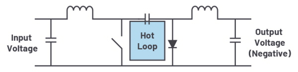
▲그림 1 : Ćuk 토폴로지를 사용해서 음의 전압을 발생시키기 위한 회로 다이어그램
그림 1에서 파란색으로 표시된 핫 루프가 이 부분에 해당한다.
핫 루프라는 용어는 일단의 트레이스들이 di/dt를 빠르게 전이한다는 뜻이다.
스위칭 전류가 발생시키는 간섭을 최소화하기 위해서는 기생 인덕턴스를 되도록 작게 해야 하고, 그러기 위해서는 이 핫 루프의 크기를 되도록 작게 해야 한다.
따라서 Ćuk 컨버터를 위한 최적의 보드 레이아웃은 프리휠링 다이오드 D, 커플링 커패시터 C, 스위치 S1을 되도록 서로 가깝게 배치하는 것이다.
LT8330의 핀아웃은 바로 이러한 요구를 충족하도록 설계되었다. 그림 2는 보드 레이아웃에서 스위칭된 전류의 전원 경로 부분(핫 루프)을 보여준다.
이 루프는 외부 다이오드 D, 커플링 커패시터 C, 그리고 LT8330 스위칭 레귤레이터 IC 내에서 GND와 SW 핀 사이의 내부 배선으로 이루어진다.
그러므로 핫 루프가 되도록 컴팩트하게 설계되었다.
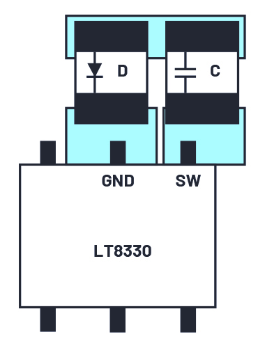
▲그림 2 : Ćuk 토폴로지의 최적화된 보드 레이아웃
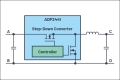
그림 3은 Ćuk 토폴로지에 적합한 레귤레이터로서 LT8330을 사용한 회로를 예시한 것이다.
이 레귤레이터의 중요한 특징은 FBX 핀이다.
이는 특수한 타입의 FB 핀으로서, Ćuk 토폴로지에서 요구하는, 음의 전압과 양의 전압을 모두 처리할 수 있다.
LT8330을 부스트나 SEPIC 토폴로지로 사용할 때는 양의 피드백 핀 극성이 필요하다.
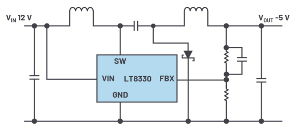
▲그림 3 : LT8330을 사용한 Ćuk 레귤레이터 회로 예시
레귤레이터의 입력 측과 출력 측 양쪽 모두의 인덕턴스가 전도 방사 양에 영향을 미친다.
핫 루프를 컴팩트하게 설계해서 최적화된 보드 레이아웃을 구현함으로써 잡음이 매우 낮은 솔루션을 달성할 수 있다.
이러한 점에서 Ćuk 레귤레이터는 저잡음 음의 전압을 발생하도록 사용하는 데 적합하다.
※ 저자 : 프레데릭 도스탈(Frederik Dostal) FAE / 아나로그디바이스(Analog Devices, Inc.)
프레데릭 도스탈(Frederik Dostal)은 독일 뉘른베르크 에를랑겐 대학에서 미세전자공학을 전공했다. 2001년 전력 관리 사업부에서 경력을 시작했으며, 애리조나주 피닉스에서 4년 간 스위치 모드 전원 공급장치를 담당하는 등 다양한 애플리케이션 직책을 맡았다. 2009년 아나로그디바이스에 입사하여 현재는 뮌헨 소재 아나로그디바이스에서 전력 관리를 위한 필드 애플리케이션 엔지니어(FAE)로 근무하고 있다.(문의 : frederik.dostal@analog.com)
.jpg)


