기사입력 2024.01.17 08:40
ST마이크로일렉트로닉스(이하 ST)가 STM32CubeMP13을 이용해 간단한 소형 MCU용으로 설계된 기존 코드를 마이그레이션하면서 고성능 MPU의 추가 기능을 차세대 제품에 활용할 수 있도록 하는 새로운 소프트웨어 팩을 무료로 제공한다.
2024-01-10 오후 3:04:42by 성유창 기자
UNIST(총장 이용훈) 에너지화학공학과 류정기 교수와 KAIST(총장 이광형) 신소재공학과 서동화 교수 공동연구팀이 높은 효율과 안정성을 가진 고순도의 그린수소 생산용 이기능성(Bifunctional) 수전해 촉매를 개발했다.
2024-01-11 오후 3:55:13by 배종인 기자

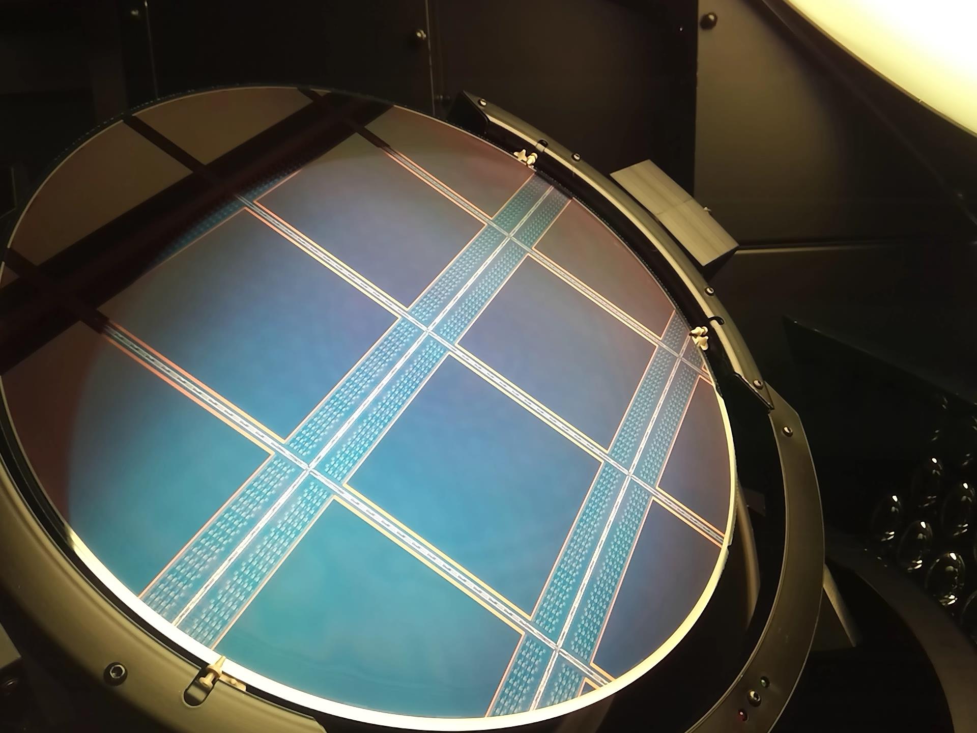
케이던스 디자인 시스템즈(Cadence Design Systems, Inc.)는 삼성 파운드리가 ‘케이던스 퀀터스 엑스트랙션(Cadence Quantus Extraction) 솔루션’과 ‘템퍼스 타이밍(Tempus Timing) 솔루션’을 활용해 삼성 5LPE 기술을 바탕으로 한 5G 네트워킹 SoC의 테이프아웃(Tape-out: 설계를 마치고 공정으로 넘어가는 단계)에 성공했다고 12일 밝혔다.
2024-01-12 오후 1:42:09by 김예지 기자
.jpg)
아나로그디바이스(ADI)가 업계 유일의 특정 목적용 풀 스택 인공지능(AI) 플랫폼 제조사인 삼바노바 시스템즈(SambaNova Systems)와 글로벌 AI 혁신을 주도하고 AI를 전사적으로 확대하기 위해 삼바노바 스위트(SambaNova Suite)를 배포한다.
2024-01-12 오후 2:39:24by 배종인 기자
ST마이크로일렉트로닉스(STMicroelectronics, 이하 ST)가 MasterGaN1L과 MasterGaN4L을 출시했다고 15일 밝혔다.
2024-01-15 오후 4:51:40by 권신혁 기자

[열린보도원칙] 당 매체는 독자와 취재원 등 뉴스이용자의 권리 보장을 위해 반론이나 정정보도, 추후보도를 요청할 수 있는 창구를 열어두고 있음을 알려드립니다.
고충처리인 장은성 070-4699-5321 , news@e4ds.com