반도체 소자 내 배선 간격, 지금보다 더 줄일 수 있어
기사입력 2020.06.25 11:20
반도체 내부 전기 간섭 최소화하는
소재 개발로 집적도 향상 가능해져
반도체 칩 안의 소자를 더 작게 만들 수 있는 소재가 국내에서 개발됐다.
울산과학기술원(UNIST) 자연과학부 신현석 교수팀이 삼성전자 종합기술원의 신현진 전문연구원팀, 기초과학연구원(IBS) 등과 국제공동연구를 통해 반도체 소자를 더 미세하게 만들 수 있는 ‘초저유전율 절연체’를 개발하는 데 성공했다.
유전율이란 외부 전기장에 반응하는 민감도를 의미한다. 유전율이 낮으면 전기적 간섭이 줄어들어 반도체 소자 내 금속 배선의 간격을 줄일 수 있다.
절연체는 전류가 흐르지 않는 물질을 의미한다. 보통 반도체 소자 내 금속 배선에서 전자가 다른 부분으로 이탈하는 것을 막기 위해 전자이동경로 사이에 절연체를 삽입한다.
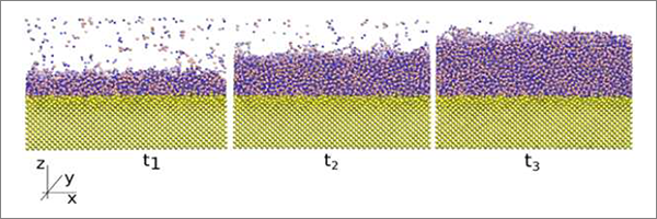
▲ 실리콘 기판 (노란색) 위에서 붕소 및 질소의 증착으로
3nm a-BN 박막이 형성되는 과정 [그림=과기정통부]
3nm a-BN 박막이 형성되는 과정 [그림=과기정통부]
반도체 소자의 크기를 줄이면서 데이터 처리 속도를 높이는 방법의 하나가 절연체의 유전율을 낮추는 것이다. 공동 연구팀은 기존 절연체보다 30% 이상 낮은 유전율을 갖는 ‘비정질 질화붕소(amorphous boron nitride) 소재’를 합성하는 데 성공했다.
과학기술정보통신부와 UNIST는 이번 성과가 네이처(Nature, IF 43.070)에 한국시각으로 6월 25일 0시 게재되었다고 밝혔다.
현재 반도체 공정에서 사용되는 절연체는 다공성 유기규산염(p-SiCOH)으로 유전율이 2.5 수준이다. 이번에 연구팀이 합성한 비정질 질화붕소의 유전율은 1.78로, 기술적 난제로 여겨진 유전율 2.5 이하의 신소재를 발견한 것이다.
연구팀은 이론적 계산 및 포항가속기연구소 4D 빔라인을 활용해 비정질 질화붕소의 유전율이 낮은 이유가 원자 배열의 불규칙성 때문이라는 점도 밝혀냈다.
또한, 기존에는 유전율을 낮추기 위해 소재 안에 미세한 공기 구멍을 넣어 강도가 약해지는 문제가 있었으나, 비정질 질화붕소는 물질 자체의 유전율이 낮아 이러한 작업 없이도 높은 기계적 강도를 유지할 수 있게 되었다.
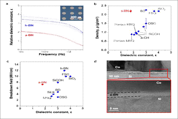
▲ 개발된 소재의 데이터와 이미지 [그림=과기정통부]
제1 저자인 홍석모 UNIST 박사과정 연구원은 “낮은 온도에서 육방정계 질화붕소(화이트 그래핀)가 기판에 증착되는지 연구하던 중 비정질 질화붕소의 유전율 특성을 발견했고, 반도체 절연체로써 적용 가능성을 확인했다”라고 밝혔다.
교신저자인 신현석 UNIST 교수는 “이 물질이 상용화된다면 중국의 반도체 굴기와 일본의 수출 규제 등 반도체 산업에 닥친 위기를 이겨내는 데 큰 도움이 될 것”이라며 “‘반도체 초격차 전략’을 이어갈 수 있는 핵심 소재기술”이라고 강조했다.
이번 연구에는 유럽연합의 그래핀 연구 프로젝트(Graphene Flagship) 파트너인 영국 케임브리지 대학교 매니쉬 초왈라 교수와 스페인 카탈루냐 나노과학기술연구소 스테판 로슈 교수가 참여했다.
연구 수행은 과학기술정보통신부의 기초연구실, 중견연구(전략) 및 기초과학연구원(IBS), 삼성전자의 지원으로 이루어졌다.
이수민 기자
관련뉴스
-

인간 두뇌 모방한 뉴로모픽 반도체, 저전력 고성능 AI 프로세싱의 열쇠
AI가 기업의 비즈니스에 활용되면서 AI 가속기에 대한 관심도 늘고 있다. 가속기에는 CPU, GPU, FPGA, ASIC 등의 프로세서가 사용된다. 그러나 무어의 법칙이 한계에 이르면서 극적인 성능 향상이나 전력 효율 상승 등을 기대할 수 없게 됐다. 이에 등장한 개념이 바로 뉴로모픽 반도체다.
2020-06-09 오후 6:21:13by 이수민 기자
-
메모리·이미지·파워 반도체 장비 투자 급증 조짐 보여
SEMI의 세계 팹 전망 보고서에 따르면, 2021년 반도체 팹 장비 투자액은 2020년 대비 약 24% 증가한 677억 달러에 이를 전망이다. 메모리 팹이 300억 달러 규모로 가장 큰 투자를 할 것으로 보이며, 로직 팹 및 파운드리가 290억 달러로 그 뒤를 이을 것으로 보인다.
2020-06-10 오후 1:01:50by 강정규 기자
-

삼성전자, 韓 팹리스에 칩 설계 플랫폼 SAFE-CDP 지원
삼성전자가 국내 시스템반도체 생태계의 경쟁력을 강화하기 위해 국내 중소 팹리스에 클라우드에서 반도체 칩을 설계할 수 있는 플랫폼인 SAFE-CDP를 지원한다고 밝혔다. SAFE-CDP는 팹리스 고객들이 아이디어만 있으면 즉시 칩 설계를 시작할 수 있도록 가상 설계 환경을 제공하는 서비스다.
2020-06-19 오전 8:31:10by 이수민 기자



많이 본 뉴스

[열린보도원칙] 당 매체는 독자와 취재원 등 뉴스이용자의 권리 보장을 위해 반론이나 정정보도, 추후보도를 요청할 수 있는 창구를 열어두고 있음을 알려드립니다.
고충처리인 장은성 070-4699-5321 , news@e4ds.com