ACM은 반도체 후공정(OSAT)업체들의 솔루션 기술 첨단화를 위해 다양한 습식 웨이퍼 공정용 제품군을 발표했다. 고객의 요구사항에 최적화된 ACM의 첨단 습식 웨이퍼 공정용 제품은 Cu 필라, Au 범핑, TSV, 팬아웃(Fan-out)과 같은 최신의 반도체 패키징 공정을 지원하며 코팅, 현상, 도금, 평탄화, 포토레지스트 스트립과 에칭과 같은 반도체 공정 전반에 걸쳐 활용이 가능하다.
최신의 반도체 패키징 공정을 지원
세계 반도체 패키징 시장, 2025년 420억 달러 예상
ACM은 반도체 후공정(OSAT)업체들의 솔루션 기술 첨단화를 위해 다양한 습식 웨이퍼 공정용 제품군을 27일 발표했다.
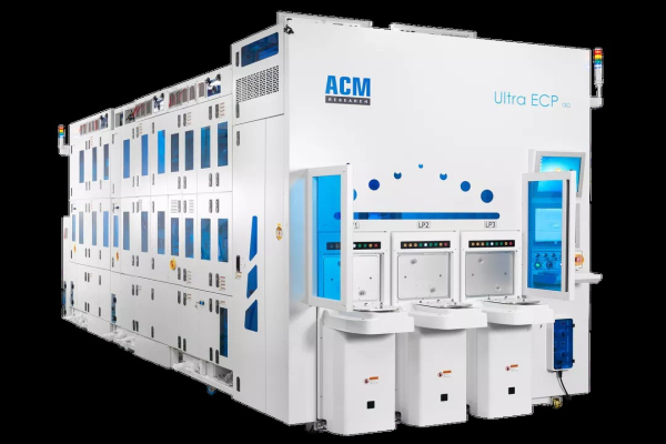
▲ ACM Ultra ECP [사진=ACM]
고객의 요구사항에 최적화된 ACM의 첨단 습식 웨이퍼 공정용 제품은 Cu 필라, Au 범핑, TSV, 팬아웃(Fan-out)과 같은 최신의 반도체 패키징 공정을 지원하며 코팅, 현상, 도금, 평탄화, 포토레지스트 스트립과 에칭과 같은 반도체 공정 전반에 걸쳐 활용이 가능하다.
반도체 시장 조사기관인 Yole Dévelopment에 따르면, 전 세계 반도체 패키징 시장규모는 2019년에290억 달러였으며 6.6%의 연평균 성장률(CAGR)로 성장해 2025년에는 420억 달러로 이를 것으로 예상된다.
전체 패키징 시장에서 첨단 패키징이 차지하는 비중 또한 무어의 법칙 둔화, 기종간의 통합, 5G, 인공 지능(AI), 고성능 컴퓨팅(HPC) 및 사물 인터넷(IoT)과 같은 새로운 분야에서 기술혁신에 대한 요구가 높아지면서 2019 년 42.6 %에서 2025 년 49.4 %로 증가될 것으로 예상된다.
ACM Research의 웨이퍼 레벨 패키징용 습식 웨이퍼 공정용 제품들은 200mm와 300mm웨이퍼에 모두 호환되며 다음과 같은 공정에서 구현할 수 있다.
ECP (Electrochemical plating)
ACM에서 자체 개발한 ECP ap 시스템은 5 % 미만의 웨이퍼 균일도, 3 % 미만의 웨이퍼 간 균일도, 2 % 미만의 재현성 및 다이 내 2.0µm 미만의 동일 평면성을 구현한다. 또한 이 시스템은 최대 3개의 로드 포트, 최대 4개의 진공 프리 웨트 챔버, 최대 20개의 도금 챔버 및 최대 4 개의 포스트 클리닝 챔버로 구성할 수 있다. ACM의 ECP 장치는 Cu, Ni, Sn/Sn-Ag 필라, 솔더 범프, Au범프 및 Cu RDL등 WLP 도금 단계에서 고객 요구 사항에 맞춰 쉽게 커스터마이즈가 가능하다. 또한 ACM의 독점적인 확산 플레이트와 특허 받은 고무씰로 인해 Fan-out, TSV, TMV(Through-Mold Via) 공정에 적합하다.
SFP(Stress-Free Polishing)
전기 화학 반응 메커니즘을 기반으로 하며 기계적 피로를 유발하지 않고 구리 및 상부barrier층을 제거하는 데 이상적이며, 화학적 기계적 연마, 습식 에칭 및 건식 에칭 공정을 통합하여 수행한다. 전해액 및 습식 에칭액 등의 화학 물질은 실시간으로 재활용 및 재사용되어 CMP 공정에서 Slurry 사용량을 80 % 이상 줄여준다.
코터(Coater)
WLP 리소그래피 공정에서 포토 레지스트와 폴리이미드 코팅, 소프트 베이크, 기상 증착을 위한 헥사메틸디실록산(HMDS) 도포와 같은 중요한 단계를 수행한다. 이 시스템은 혁신적인 방법과 정밀한 코팅 제어를 사용하여 정밀한 가장자리 장벽 제거를 달성할 수 있다. 구성은 ACM 고유의 자동 세척 기능이 있는 최대 4개의 코팅 챔버, 다양한 종류의 포토레지스트 노즐 중 하나 또는 두 개, 8~14개의 핫 플레이트, 2~4개의 콜드 플레이트, 그리고 1 또는 2개의 HMDS 자동 클리닝 챔버와 같은 옵션으로 사용자 지정이 용이하다. ACM의 독점적인 코팅 챔버의 자동 세척 기술은 특히 100µm 이상의 높은 두께의 포토레지스트 코팅 공정에서 예방 정비 시간을 단축시킬 수 있다.
디벨로퍼(Developer)
ACM의 디벨로퍼 시스템은 노광 후 베이크, 현상 그리고 하드 베이킹 기능을 위해 설계되었으며, 3가지 PR 현상 방법과 양면 공정을 지원한다. 이 시스템은 각각 1~5개의 액체 노즐 세트를 포함하는 최대 4개의 현상 챔버 세트로 구성할 수 있으며, 사용자는 2~14 개의 핫 플레이트와 2~4 개의 콜드 플레이트 중에서 선택할 수 있다.
습식 에처(Wet etcher)
ACM의 습식 에칭 시스템은 다양한 화학 물질을 사용하여 웨이퍼에서의 과잉 언더 범프 메탈을 제거하며 스마트-시퀀스 레시피 기능을 통해 Cu 및 티타늄(Ti) 에칭과 같은 금속 에칭 프로세스를 결합할 수 있다. 이것은 하나의 시스템에서 예정된 순서로 수행될 수 있다. 시스템은 4개 또는 8개의 단일 웨이퍼 식각 챔버로 사용자 요구에 맞춰 커스터마이즈할 수 있고 최대 5개의 화학 물질을 다룰 수 있으며 양면 공정 및 두 가지 화학물질의 재사용이 가능하다.
포토레지스트 스트립(Photoresist strip)
PR 제거를 위해 설계된 고효율의 ACM의 습식 제거 시스템은 1개의 통합 탱크와 4개의 싱글 웨이퍼 챔버를 갖춘 하나의 장비에서 벤치 소킹과 싱글 스핀 PR 제거 프로세스를 수행한다. 우선 웨이퍼는 처리속도 향상을 위해 한 번에 여러 웨이퍼를 보유하는 용매 탱크에 담그고 다음으로, 웨이퍼 제어를 강화하기 위해 싱글 웨이퍼 모듈로 옮겨지고 회전하는 웨이퍼에 화학 물질이 분사된다. 싱글 스트립 챔버는 양면 공정을 수행하고 두 가지 화학 물질의 재사용이 가능하다. 싱글 스트립 챔버에서 잔류물 제거를 지원하는 SAPS 메가소닉(Megasonic)은 제품 수율을 향상시키기 위해 중요한 스트리핑 공정에 사용할 수 있다.
스크러버(Scrubber)
ACM의 스크러버 시스템은 여러 가지 세정 방법을 사용하여 통합 칩 제조 및 웨이퍼 레벨 패키징(WLP) 공정 모두에 있어 높은 파티클 제거 효율을 달성하도록 설계되었다. 고압 탈이온수를 이산화탄소(CO2)와 혼합해 액상과 가스상 화학물질을 모두 결합한 이중유체 스프레이 세정제를 만든다. 또한 부드러운 브러시를 사용하면 크기가 다른 파티클들을 제거할 수 있다. 이 시스템은 ACM 고유의 SAPS 메가소닉 클리닝 기술과 양면 세정을 위한 웨이퍼 플립 기능을 추가할 수 있다. 스크러버 시스템은 실리콘 및 유리 기판는 물론 접합 웨이퍼와도 호환이 가능하다. 4 챔버 스크러버 시스템은 시간당 100매의 웨이퍼 처리가 가능하다.


