재료연, 뉴로모픽 반도체 구현
기사입력 2023.02.08 11:20
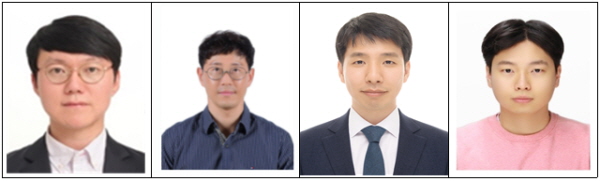
▲이번 연구를 주도한 (왼쪽부터)한국재료연구원 김용훈 선임연구원, 권정대 책임연구원, 부산대 이제인 교수, 한국재료연구원 박병진 학생연구원
정보처리·저장 동시수행, 다양한 AI디바이스 적용 기대
손글씨 패턴 이미지 학습결과 인식률 정확도 97% 기록
손글씨 패턴 이미지 학습결과 인식률 정확도 97% 기록
과학기술정보통신부 산하 정부출연연구기관인 한국재료연구원(KIMS, 원장 이정환)이 정보처리와 저장을 동시에 수행 가능해 손글씨 패턴과 같은 이미지 학습 및 인식을 수행할 수 있는 뉴로모픽 반도체 소자를 세계 최초로 구현해 향후 다양한 인공지능 디바이스에 적용될 수 있을 것으로 기대를 모으고 있다.
재료연구원은 나노표면재료연구본부 김용훈, 권정대 박사연구팀이 리튬이온 배터리 핵심 소재인 리튬이온을 박막화해 고집적, 고신뢰성을 가진 차세대 뉴로모픽 반도체 소자를 세계 최초로 구현하는 데 성공했다고 8일 밝혔다.
이 기술은 최근 주목받고 있는 리튬이온 배터리의 핵심 소재인 리튬이온을 초박막화해 이를 2차원 나노소재와 접목함으로써, 고집적이 가능하면서도 고신뢰성을 가진 차세대 인공지능 반도체 핵심 소자 제조 기술이다.
뉴로모픽 반도체 소자는 인간의 뇌와 유사하게 시냅스와 뉴런으로 구성된다. 이때 정보처리와 저장기능을 동시에 수행하는 시냅스 소자의 개발이 필수이다.
시냅스 소자는 인간의 뇌와 유사하게 뉴런의 신호를 받아 시냅스 가중치(연결 강도)를 다양하게 변조해 정보의 처리와 기억을 동시에 수행하는 특징을 가진다.
특히 시냅스 가중치의 선형성과 대칭성을 만족하면 다양한 패턴인식을 손쉽게 저전력으로 구현할 수 있다는 장점이 있다.
기존 연구는 주로 이종(異種) 물질의 계면 사이에 전하 트랩을 이용하거나, 산소 이온 등을 이용해 시냅스 가중치를 조절했다.
반면에 이 경우, 외부 전계에 따라 이온의 이동을 원하는 대로 조절하기 어렵다는 단점이 있었다.
연구팀은 리튬이온의 외부 전계에 따른 이동성을 유지하면서 동시에 박막화 공정개발을 통해 고집적 인공지능 반도체 소자를 개발해 이 문제를 해결했다.
수십 나노미터 두께의 박막화로 웨이퍼 스케일의 두께 조절과 미세패턴 공정이 가능해 기존 반도체 공정에 적합하다는 장점이 있다.
연구팀은 일반적인 반도체 공정에 사용되는 진공 스퍼터링(Vacuum Sputtering) 증착 방식을 이용해 리튬이온의 박막화에 성공했다.
이때 증착되는 리튬이온 박막의 두께는 100나노미터 이하 수준이다. 이후 반도체 공정을 통해 트랜지스터 형태의 소자를 실리콘 웨이퍼 기판상에 만들고 외부에서 전계를 가하면 전하를 띤 리튬 박막 안의 리튬이온이 가역적으로 움직여 채널의 전도도를 세밀하게 조절할 수 있게 된다.
연구팀은 이렇게 개발된 시냅스 소자를 이용해 인공신경망 학습패턴을 구현하고, 이를 바탕으로 손글씨 이미지 패턴인식을 학습했다. 제작된 인공지능 반도체 소자는 미세하게 조절되는 시냅스 가중치 특성을 500회 이상의 반복되는 전계에도 유지함으로써 약 96.77%라는 높은 손글씨 패턴 인식률을 보였다.
김용훈, 권정대 박사연구팀은 “이번에 개발된 차세대 뉴로모픽 반도체 소자는 기존 폰노이만 방식의 정보처리장치인 CPU와 정보저장장치인 메모리를 각각 필요로 하지 않고, 정보처리와 저장을 동시에 수행하며 손글씨 패턴과 같은 이미지 학습 및 인식을 수행할 수 있다”며 “향후 세계적 수준의 뉴로모픽 하드웨어 시스템, 햅틱 소자, 비전 센서 등 다양한 저전력 인공지능 디바이스에 확대 적용될 것으로 기대된다”고 말했다.
한편 이번 연구성과는 과학기술정보통신부의 지원을 받아 한국재료연구원 주요사업과 한국연구재단 소재혁신선도프로젝트 사업을 통해 수행됐다.
또한 연구 결과는 세계적인 학술지인 에이씨에스(ACS)에서 발행하는 ‘에이씨에스 에이엠아이(ACS AMI, ACS Applied Materials & Interfaces, IF: 10.383)’에 2022년 11월 17일자로 게재됐다.(제1저자: 박병진 학생연구원, 공동교신: 부산대 이제인 교수)
현재 연구팀은 이번 연구 결과를 저전력 인공지능 디바이스 및 웨어러블 엣징 디바이스에 적용해 지능형 웨어러블 디바이스 분야에 관한 후속 연구를 진행 중이다.
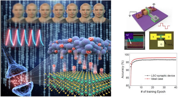
▲배터리소재를 접목한 고집적, 고신뢰성의 차세대 뉴로모픽 반도체 소자 모식도(좌), 리튬이온 소재를 박막화하여 고집적의 3단자 기반 소자 사진 및 손글씨 패턴 정확도(우)

관련뉴스
-
.JPG)
재료硏, 제우스에 고감도 나노플라즈모닉 센서 기판 제조기술 이전
한국재료연구원(KIMS, 원장 이정환)이 반도체·디스플레이·로봇 제조 전문기업인 ㈜제우스에 고감도 나노플라즈모닉 센서 기판 제조기술을 이전하며, 전기전자제품의 환경유해물질(RoHS) 규제 대응에 나선다.
2022-10-04 오전 10:44:30by 배종인 기자
-
스마트 윈도우 산업 활성화 본격화
과학기술정보통신부 산하 정부출연연구기관인 한국재료연구원(KIMS, 원장 이정환)이 10일 건국대 서울캠퍼스에서 ‘제1회 스마트 윈도우 산업기술교류회’를 개최했다.
2023-01-11 오전 9:02:48by 배종인 기자
-
.jpg)
재료연 ㈜트윈위즈, 투자 22억 확보 미래 가치 인정
과학기술정보통신부 산하 정부출연연구기관인 한국재료연구원(KIMS, 원장 이정환)의 연구소기업인 ㈜트윈위즈가 투자 혹한기 속에서 창업 1년도 채 되지 않아 20억원 규모의 프리 시리즈 A투자를 유치했다.
2023-01-11 오전 9:21:03by 배종인 기자


많이 본 뉴스
[열린보도원칙] 당 매체는 독자와 취재원 등 뉴스이용자의 권리 보장을 위해 반론이나 정정보도, 추후보도를 요청할 수 있는 창구를 열어두고 있음을 알려드립니다.
고충처리인 장은성 070-4699-5321 , news@e4ds.com