인피니언 상단면 냉각 패키지, JEDEC 표준 등록
기사입력 2023.02.14 15:25
새로운 애플리케이션 디자인에 상단면 냉각 패키지 채택 가속화
TO247·TO220 대체…상단면 냉각 기술 시장 도입 ↑
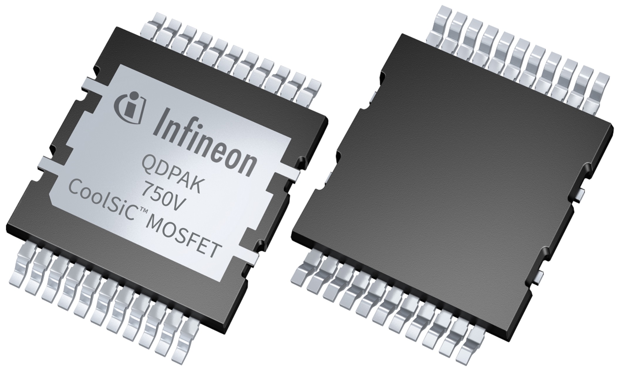
인피니언 테크놀로지스(이하 인피니언)가 TO247과 TO220보다 두 배 이상 전력 밀도를 향상시키고 BOM을 줄여 전반적인 시스템 비용을 낮춘 상단면 냉각(TSC) 패키지를 JJEDEC 표준으로 등록했다.
인피니언은 고전압 MOSFET에 이상적인 자사의 QDPAK 및 DDPAK 상단면 냉각(TSC) 패키지를 JEDEC 표준으로 등록했다고 14일 밝혔다.
전기차를 위한 효율적인 고전력 애플리케이션을 개발하기 위해서 전력 밀도와 비용 최적화가 갈수록 더 중요해지고 있다.
이제 하나의 표준 패키지와 풋프린트로 새로운 애플리케이션 디자인에 상단면 냉각 패키지의 광범위한 채택을 가속화하게 되었다.
또한 OEM 제조사들에게 자사 제품을 차별화할 수 있는 유연성을 제공하며 다양한 애플리케이션에서 전력 밀도를 한 차원 끌어올리도록 한다.
JEDEC는 50년 넘는 역사를 자랑하는 표준화 기구로 마이크로일렉트로닉스 업계를 위해서 패키지 아웃라인을 비롯한 다양한 기술들과 관련해서 공개 표준과 문헌을 개발해 왔다.
JEDEC는 TO220과 TO247 쓰루홀 디바이스(THD) 같은 반도체 패키지를 폭넓게 수용해 왔다.
지난 수십 년간 이들 패키지가 주로 사용되어 왔으며, 최신 온보드 차저(OBC) 디자인이나 고전압(HV) 및 저전압(LV) DC-DC 컨버터에 지금도 사용되고 있다.
이제 QDPAK 및 DDPAK 표면 실장(SMD) 상단면 냉각 패키지를 표준으로 등록함으로써 각각 TO247과 TO220을 대체하는 상단면 냉각 기술의 광범위한 시장 도입을 가속화하게 되었다.
인피니언은 고객들이 TO220 및 TO247 THD 디바이스를 QDPAK 및 DDPAK SMD 디바이스로 쉽게 전환할 수 있도록 동일한 열 성능으로 향상된 전기적 성능을 제공하도록 이들 디바이스를 설계했다.
QDPAK 및 DDPAK SMD 상단면 냉각 패키지의 표준 높이 2.3mm를 기준으로, 개발자들은 이제 동일한 높이의 SMD 상단면 냉각 디바이스들을 사용해서 OBC나 DC-DC 변환 등의 애플리케이션을 설계할 수 있게 되었다.
따라서 3D 냉각 시스템을 필요로 하는 기존 솔루션과 비교해서 설계가 수월하고 냉각을 위한 시스템 비용을 줄일 수 있다.
뿐만 아니라 상단면 냉각 패키징은 표준 하단면 냉각(BSC)에 비해서 열 저항이 최대 35퍼센트 더 낮다.
상단면 냉각 패키지는 PCB 양면을 모두 사용할 수 있도록 하므로 보드 공간 활용도를 높이고 최소 두 배 이상 전력 밀도를 향상시킨다.
서브스트레이트에서 열적으로 분리됨으로써 패키지 열 관리 또한 향상시킨다.
노출된 패키지 상단면에 비해서 리드의 열 저항이 훨씬 높기 때문이다.
열 성능이 향상됨으로써 보드들을 적층할 필요가 없어진다. FR4와 IMS를 함께 사용할 필요 없이, 모든 부품들을 탑재하기 위해서 단일 FR4로 충분하며 커넥터 또한 적게 필요하다.
따라서 BOM(bill of materials)을 줄여 전반적인 시스템 비용을 낮춘다.
열 성능과 전력 용량 향상뿐만 아니라, 상단면 냉각 기술은 전력 루프 설계를 최적화해서 신뢰성을 높일 수 있다.
이것은 드라이버를 전력 스위치에 아주 가깝게 배치하는 것으로써 가능하다.
드라이버 스위치 루프의 낮은 부유 인덕턴스가 루프 기생성분을 줄이고, 이것은 게이트에 링잉을 낮추고 성능을 높이고 결함 위험을 줄인다.


많이 본 뉴스
[열린보도원칙] 당 매체는 독자와 취재원 등 뉴스이용자의 권리 보장을 위해 반론이나 정정보도, 추후보도를 요청할 수 있는 창구를 열어두고 있음을 알려드립니다.
고충처리인 장은성 070-4699-5321 , news@e4ds.com