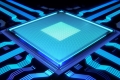
과학기술정보통신부는 한국과학기술원(KAIST) 유회준 교수 연구팀이 국내 최초로 DRAM 메모리 셀 내부에 직접 연산기를 집적해 AI 연산을 수행하는 PIM 반도체인 ‘다이나플라지아(DynaPlasia*)’를 개발했다.
▲국내 연구진이 국내 최초 아날로그형 DRAM-PIM을 개발했다.
DRAM-PIM ‘다이나플라지아’…집적도·연산 성능↑
1개 메모리 셀, 메모리·연산기·데이터 변환 지원
국내 연구진이 국내 최초 아날로그형 DRAM-PIM 기반 AI 반도체를 개발해 최근 챗GPT 등 거대해지는 AI 모델 시장 선점에 기여할 것으로 기대된다.
과학기술정보통신부는 한국과학기술원(KAIST) 유회준 교수 연구팀이 국내 최초로 DRAM 메모리 셀 내부에 직접 연산기를 집적해 AI 연산을 수행하는 PIM 반도체인 ‘다이나플라지아(DynaPlasia*)’를 개발했다고 밝혔다.
PIM(Processing-in-Memory)은 하나의 칩 내부에 메모리와 프로세서를 통합해 데이터 처리를 수행하는 기술이다. 메모리와 프로세서가 분리되어 있는 기존 컴퓨팅 구조(폰 노이만 구조, Von Neumann Architecture)에서 발생하는 데이터 병목현상 및 과다한 전력 소모 문제를 해결할 수 있어 차세대 AI 반도체의 히든카드로 떠올랐다.
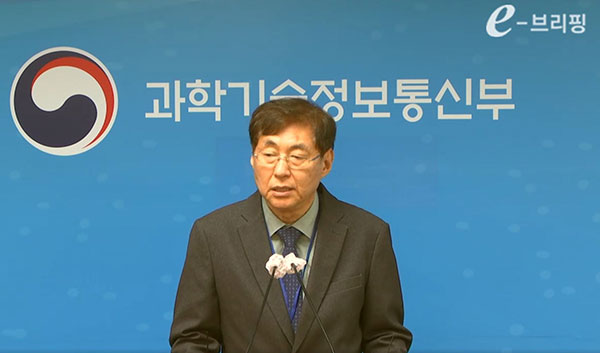
유회준 KAIST ICT석좌교수는 14일 PIM 반도체 관련 연구성과 브리핑에서 "그 동안 TSMC에서 주도를 했지만, 메모리 강국인 우리나라가 주도로 메모리가 중심이 돼야 한다는 생각에 삼성, SK하이닉스를 필두로 연구해왔다"고 말했다.
또한 이번 연구 성과에 대해 "하지만 지난 PIM들은 궁극적인 PIM이라기보다는 PNM, 즉 Process-In-Memory가 아니라 Process-Near-Memory의 형태를 취하고 있었고, 이번에 발표한 것이 진정한 PIM, 프로세서가 메모리 안에 들어 있는 그런 구조"라고 말했다.
특히 "프로세서만이 아니라 메모리 기능도 하고, 아날로그 컴퓨팅 방식이며, 셀 하나가 메모리도 되고 프로세서도 되고 ADC용 캐패시터도 되는 ‘트리플-모드’라는 이름을 붙였다"고 말했다.
유 교수에 따르면, 기존에도 PIM 반도체가 개발되기는 했지만, 대부분 셀 하나에 8개 이상의 트랜지스터가 필요한 SRAM-PIM 방식이거나, 기존 PIM과 같이 DRAM 기반 PIM으로 구현되었더라도 연산기를 메모리 셀 어레이의 내부가 아닌 외부에 근접하게 배치하는 디지털 PIM(Near Memory PIM) 방식이었다.
이러한 디지털 PIM 방식은 메모리와 연산기 사이의 거리를 줄이고 대역폭을 넓혀 데이터 병목현상은 감소시키지만, 메모리 셀 내부에 직접 연산기를 집적하여 연산 성능을 올리지는 못했다.
이번에 연구팀이 발표한 ‘다이나플라지아(DynaPlasia)’는 전체 하드웨어 구조를 최적화했다. 아날로그형 DRAM-PIM 기반 AI 반도체로, 3개의 트랜지스터만으로 셀을 구성했으며, 메모리 셀 내부에 연산기를 집적하고, 아날로그 연산 방식을 이용해 집적도와 연산기능을 향상시켰다. 내부 곱셉 로직에서 누설전류를 제거한 내성 컴퓨팅을 통해 모든 메모리 셀들이 병렬로 동작할 수 있도록 했다.
결국 기존 디지털 DRAM-PIM 방식 대비 약 300배 높은 병렬성으로 15배 높은 데이터 처리량을 보인다는 설명이다.
또한 기존 아날로그형 PIM 반도체에서는 메모리와 연산기, 데이터 변환기를 별도로 구현해 고정된 하드웨어 구조를 사용했으나, 이번 연구에서는 하나의 셀이 메모리, 연산기, 데이터 변환기의 기능을 동시에 지원할 수 있는 ‘트리플-모드 셀’을 개발했다.
‘트리플-모드 셀’을 통해 실제 AI 연산에 맞춰 하드웨어 구조를 형성하는 동적 코어 형성 아키텍처로 기존 아날로그형 PIM 반도체보다 2.5배 가량 높은 효율성을 얻을 수 있다.
한편 이번 연구는 과기정통부 ‘PIM인공지능반도체핵심기술개발(설계)’ 사업을 통해 설립된 ‘PIM반도체 설계연구센터(이하 ‘PIM-HUB’)’에서 진행됐으며, 지난달 미국 샌프란시스코에서 개최된 국제고체회로설계학회(ISSCC)에서 발표됐다.
작년 6월 개소한 ‘PIM-HUB’는 삼성전자와 SK하이닉스가 운영위원으로 참여하며 상호 인력파견 및 공동연구 수행, 인력양성을 위한 교육과정 공동개발 등 인력교류를 추진하고 있다.
KAIST 유회준 전기및전자공학부 교수는 “이번 연구는 기존 인공지능 반도체가 가지고 있던 메모리 병목현상을 해소할 뿐만 아니라, 높은 처리량과 가변성을 갖는 고메모리 용량의 DRAM-PIM을 개발했다는 점에서 의미가 크다. 본격적인 상용화에 성공할 경우, 최근 더욱 거대해지고 다양해지는 인공지능 모델에서도 높은 성능을 보일 수 있을 것”이라고 연구의 의의를 설명했다.
과기정통부 전영수 정보통신산업정책관은 “PIM반도체 기술은 메모리 반도체 기술에 강점을 보유한 우리나라가 앞서나갈 수 있는 잠재력이 높은 분야”라며, “글로벌 최고 수준의 초고속·저전력 인공지능 반도체를 개발할 수 있도록 하드웨어 뿐 아니라 국산 인공지능 반도체를 데이터센터에 적용하기 위해 필요한 소프트웨어 및 클라우드 관련 기술개발까지 적극적인 지원을 아끼지 않겠다”고 밝혔다.