프랙틸리아가 프랙틸리아 오버레이 패키지(Fractilia Overlay Package)를 제공하며, EUV 패턴 제어 및 수율 향상에 나선다.
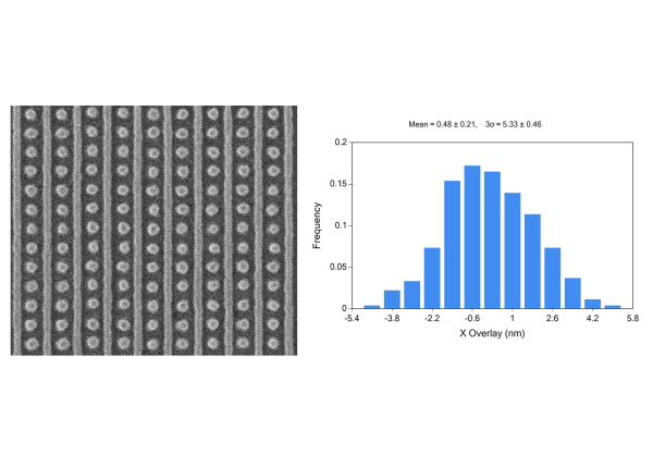
▲프랙틸리아는 오버레이 패키지는 피처들 간의 SEM 오버레이를 분석하고 오버레이 분포, 웨이퍼 간 변형 등을 계산한다.(출처: 프랙틸리아)
스토캐스틱 제어 솔루션 오버레이 패키지 제공
스토캐스틱(stochastic) 기반 분석과 제어를 이끌어가는 차세대 반도체 산업 주자인 프랙틸리아(Fractilia)가 EUV 패턴 제어 및 수율 향상을 위한 분석 기능을 제공한다.
프랙틸리아는 프랙틸리아 오버레이 패키지(Fractilia Overlay Package)를 제공한다고 26일 밝혔다.
프랙틸리아 오버레이 패키지는 프랙틸리아의 MetroLER™ 및 FAME™ 제품에 핵심적인 오버레이 측정 및 분석 기능을 새롭게 추가하는 옵션 제품이다.
MetroLER™와 FAME™은 프랙틸리아의 특허 기술인 FILM™(Fractilia Inverse Linescan Model) 기술에 진정한 컴퓨터 분석 기술을 결합한 것으로서, 첨단 노드에서 패터닝 오류의 원인으로 지목되는 모든 주요 스토캐스틱 효과를 매우 정확하고 정밀하게 측정할 수 있는 유일하게 검증된 팹 솔루션을 제공한다.
현재 다수의 반도체 칩 제조사들이 자신들의 주사전자현미경(Scanning Electron Microscope, SEM) 기반 오버레이 데이터 분석에 새로운 프랙틸리아 오버레이 패키지를 활용하기 위해 프랙틸리아와 협력하고 있다.
반도체 제조에서, 오버레이란 패터닝이 이루어진 각 레이어를 이전 단계 레이어 위에 정확히 포개 놓음으로써 디바이스가 전기적 접속이 잘 이루어지고 제대로 동작하게 하는 것을 말한다.
기존에는 칩 제조사들이 광학 기반의 측정 장비들을 사용해 이러한 패턴 오버레이를 분석 및 제어해 왔는데, 이 공정은 높은 수율로 고성능 반도체 디바이스를 생산하는 데 있어서 필수적이다.
이러한 분석은 디바이스 자체에서보다는 스크라이브 라인(scribe line)에서 특정 표적에 대해 이루어진다.
칩의 회로 선폭이 계속해서 축소되고, EUV 패터닝 도입으로 스토캐스틱 변이가 증가함에 따라, 스크라이브 라인에서 분석되는 것과 디바이스에서 실제로 일어나는 것 사이에 차이가 점점 더 벌어지고 있다.
그 결과, 광학 장비에 비해 해상도와 정밀도가 더 높은 SEM 장비를 활용해 오버레이를 분석하는 방식에 대한 관심이 높아지고 있다.
반면에 SEM은 SEM 이미지에 노이즈가 생기는데, 이 노이즈를 웨이퍼 상의 스토캐스틱 변동성으로 오인하기 쉽다.
프랙틸리아의 크리스 맥(Chris Mack) CTO는 “첨단 패터닝 공정 제어를 향상시키기 위해 SEM 기반의 오버레이 분석이 점점 더 많이 사용되고 있지만, 이 방법 역시 다른 스토캐스틱 분석 방법들과 마찬가지로 시스템 차원의 임의적 SEM 오차의 영향을 받는다”며 “프랙틸리아는 우리의 입증된 FILM 기술을 통해 SEM 노이즈를 분석 및 제거하는 데 있어서 독보적인 입지를 갖추고 있으며, 그 결과 많은 고객들이 우리의 기술을 활용해 자신들의 SEM 오버레이 분석 정확도를 향상시키기 위해서 프랙틸리아를 찾고 있다. 뿐만 아니라, 프랙틸리아 오버레이 패키지를 통해 SEM 스토캐스틱 분석과 광학 오버레이 분석을 결합하면 SEM 오버레이 분석 정확도를 향상시킬 수 있을 뿐만 아니라 더 나은 랏 배치(Lot dispositioning) 및 보정값을 구할 수 있어, 궁극적으로 패터닝 제어를 향상시키고 NZO(non-zero offset) 다시 말해 스토캐스틱 변이를 낮출 수 있을 것으로 확신한다”고 말했다.
프랙틸리아의 FAME 솔루션 포트폴리오는 고유의 물리학 기반 SEM 모델링 및 데이터 분석 접근법을 사용해서 SEM 이미지로부터 시스템 차원의 임의적 오차를 분석 및 제거하고, 이미지 상에 보이는 것이 아니라 실제 웨이퍼 상에 일어나고 있는 것을 정확히 측정하도록 한다.
FAME은 라인 에지 거칠기(LER)/라인폭 거칠기(LWR), 국소적 CD 균일성(LCDU), 국소적 에지 배치 오류(LEPE), 그리고 스토캐스틱 결함 같은 모든 주요 스토캐스틱 효과를 동시에 측정할 뿐 아니라 임계선폭(CD) 분석도 제공한다. 이는 업계에서 신호대 잡음비(SNR)가 가장 높은 에지 검출을 자랑하며(경쟁 솔루션 대비 최대 5배 더 높은 SNR), 각각의 SEM 이미지로부터 30배 이상 더 많은 데이터를 추출한다.
새로운 프랙틸리아 오버레이 패키지를 통해, 프랙틸리아는 기존의 분석 성능에 더해서 고도로 정확한 SEM 기반 오버레이 분석(스토캐스틱 특성 분석 포함)을 추가하게 됐다.
프랙틸리아의 제품은 선도적인 주요 반도체 제조사, 장비 회사, 소재 공급회사, 연구 기관 등 반도체 업계 수십 여 기업들이 채택하고 있다.


