삼성전자가 2025년 8인치 질화갈륨(GaN) 전력반도체의 파운드리 서비스를 개시하는 등 전력반도체 및 전장용 반도체 주문 생산 확대에 본격 나선다.
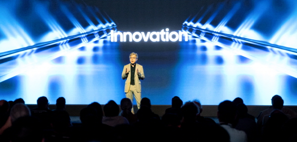
▲Samsung Electronics Foundry Business Division President Choi Si-young is giving a keynote speech at the 'Samsung Foundry Forum 2023'.
Power semiconductors and electric field expansion, full-scale mass production at Pyeongtaek Line 3
MDI Alliance-led Heterogeneous Integration Package Technology Innovation
Samsung Electronics will begin expanding its on-demand production of power semiconductors and automotive semiconductors by launching a foundry service for 8-inch gallium nitride (GaN) power semiconductors in 2025.
Samsung Electronics held the 'Samsung Foundry Forum 2023' in Silicon Valley, USA on the 27th and promised to provide expanded cutting-edge foundry process services and stable customer support through step-by-step execution of the Shell First strategy.
Samsung Electronics presented various methods to overcome the limitations of cutting-edge semiconductors in the era of artificial intelligence (AI) under the theme of ‘Innovating Beyond Boundaries.’
In particular, the company announced that it would strengthen the competitiveness of its foundry business by expanding the application of the cutting-edge 2nm process, launching the advanced package association 'MDI (Multi Die Integration) Alliance', and mass producing foundry products at its Pyeongtaek 3-line in the second half of this year.
First, Samsung Electronics specifically revealed its 2nm mass production plan and performance at this forum.
Samsung Electronics to focus on 2nm process for mobile devices in 2025(SF2) will be mass-produced and expanded to high-performance computing (HPC) processes in 2026 and automotive processes in 2027. The cutting-edge SF2 process improves performance by 12%, power efficiency by 25%, and reduces area by 5% compared to SF3.
Additionally, the 1.4 nanometer process will be mass-produced as planned in 2027.
Along with this, it will start an 8-inch GaN (gallium nitride) power semiconductor foundry service in 2025 for consumers, data centers, and automotive.
In addition, in order to secure the next-generation 6th generation mobile communication (6G) preliminary technology, a 5nm RF (Radio Frequency) process will be developed and mass-produced in the first half of 2025. The 5nm RF process improves power efficiency by more than 40% and reduces area by 50% compared to the existing 14nm process.
We plan to expand the 8nm and 14nm RF processes currently in mass production to various applications, including automotive as well as mobile.
Samsung Electronics is proactively building semiconductor cleanrooms in Pyeongtaek and Taylor to respond quickly and flexibly to market and customer demand, and the size of the cleanrooms in 2027 will be expanded 7.3 times compared to 2021.
Samsung Electronics plans to begin mass production of foundry products for various applications, including mobile, at its Pyeongtaek Line 3 in Korea in the second half of this year. In addition, the Taylor Line 1 in the US, currently under construction, is scheduled to be completed in the second half of this year as planned, and full-scale operation will begin in the second half of next year.