▲‘MOSFET의 선정 및 사용 방법’ 웨비나 중
ROHM, e4ds 웨비나서 MOSFET 기초·특성·주의점 공유
ROHM DFN·웨이퍼 레벨 칩 사이즈 패키지 시리즈 소개
ROHM(이하 로옴)이 자동차 전장화 트렌드로 증가하고 있는 MOSFET의 기초 지식, 특성과 함께 로옴의 MOSFET 제품 정보를 공유했다.
태현호 로옴 연구원은 지난 1일 e4ds에서 ‘MOSFET의 선정 및 사용 방법’을 주제로 웨비나를 갖고 MOSFET의 특성부터 고효율과 소형화를 만족하는 로옴의 신제품 DFN 시리즈 등에 대해 소개했다.
MOSFET은 바이폴라 트랜지스터에 비해 고속 스위칭과 적은 손실이 특징인 디바이스로서 자동차기기를 포함한 전자기기 및 전원 회로, 모터 구동 회로 등 폭넓은 분야에서 사용되고 있다.
ADAS로 대표되는 자동차 전장화가 한층 더 가속화됨에 따라 MOSFET의 사용 수량도 증가할 것으로 예측되고 있다.
또한 MOSFET은 최근의 환경 관련 이슈로 인한 친환경 제품의 수요 증가에 따라 손실이 적은 고효율 제품의 수요가 증가하고 있으며 다양한 기기의 전장화에 따른 공간 제약이 심해지고 있어 소형 패키지 제품에 대한 수요도 증가하고 있는 상황이다.
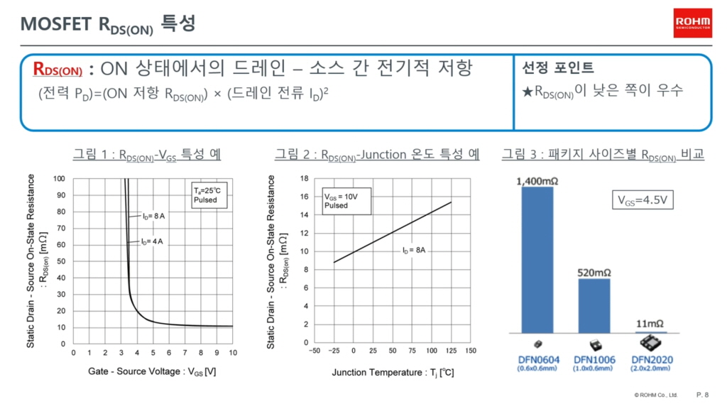
MOSFET이 ON 상태일 때 드레인-소스 간 전기적 저항치를 ON 저항이라 부르며 기호로는 RDS(ON)으로 표기고, ON 저항은 수치가 낮을수록 동작 시의 손실이 적다.
MOSFET의 ON 저항은 일반적으로 옴(Ω) 단위 이하이기 때문에 트랜지스터에 비해 저소비 전력이며, 회로 방열 대책도 간소화할 수 있다.
게이트 소스 전압도 전류에 따라 변화하는데, 전력의 손실을 개선하는 경우에는 게이트 소스 전압과 드레인 전류를 고려한 ON 저항치를 사용해 계산해야 한다.
ON 저항은 또한 온도에 따라서도 변화하기 때문에 주의가 필요하다.
일반적으로 MOSFET의 칩 크기를 크게 할수록 ON 저항치는 작아진다.
패키지의 사이즈가 클수록 탑재할 수 있는 칩의 크기도 커지기 때문에 ON 저항치가 작아지는 경향이 있다.
게이트 임계치 전압은 MOSFET가 ON이 되기 시작하는 게이트 전압을 뜻하며 기호로는 VGSth로 표기한다.
임계치 이상의 전압을 인가하면 MOSFET은 ON 상태가 된다.
MOSFET이 ON이 되는 데 필요한 전류는 제품 별로 다르기에 사양서의 전기적 특성란을 확인해야 한다.
태현호 연구원은 위의 특성 이외에도 MOSFET의 SOA(Safety Operation Area, 안전 동작 영역)과 ESD(Electro-Static Discharge, 정전기 방전) 등 다양한 특성과 주의점을 공유했다.
이어 그는 낮은 ON 저항과 고속 스위칭을 특징으로 하는 로옴의 MOSFET을 소개하며 자동차, 산업기기, 전원 모터 등 다양한 용도에 따라 선택 가능하다고 전했다.
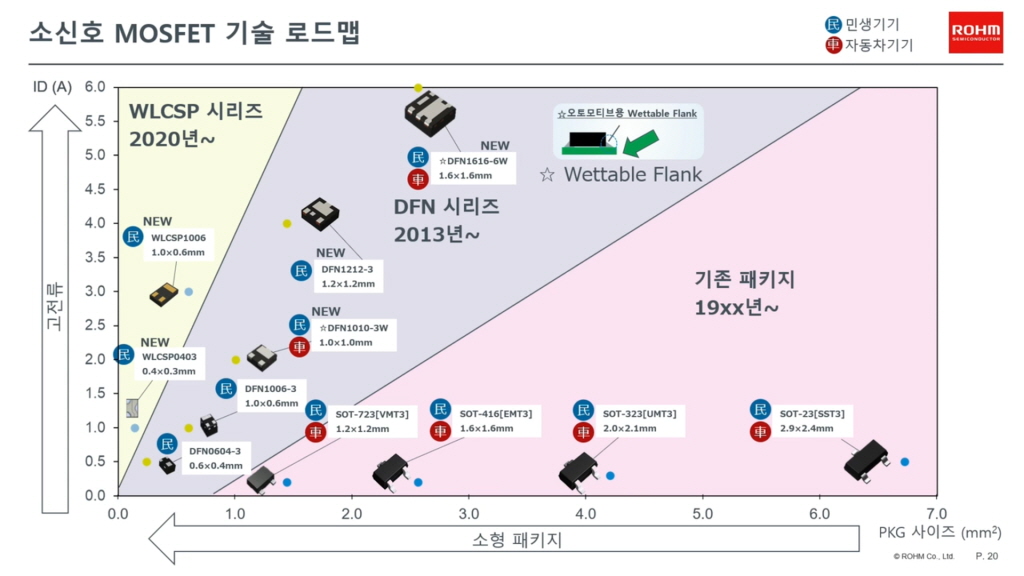
더불어 향후 시장의 요구가 증가할 것으로 예상되는 소형 고전류 제품을 위한 DFN 시리즈 제품과 CSP 타입의 웨이퍼 레벨 칩 사이즈 패키지 시리즈로 라인업을 확충해 나가고 있다.
 ▲‘MOSFET의 선정 및 사용 방법’ 웨비나 중
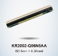
DFN 패키지 제품은 기존 리드 타입 패키지와 달리 이면 전극 제품으로 1mm x 1mm 패키지에 SOT-23과 동일한 사이즈의 칩을 탑재할 수 있어 완성품의 사이즈를 85% 줄일 수 있다.
또한 SOT-23 보다 방열성이 65% 향상되어 소형화와 고방열성을 동시에 실현해 기판의 고밀도화에도 대응 가능하다.
본래 DFN 제품은 이면 전극 제품이기에 솔더 필렛이 형성되지 않아 고신뢰성을 요구하는 오토모티브용으로는 사용되지 않았다.
로옴은 오토모티브용으로도 이를 사용할 수 있도록 Wettable Flank 가공을 도입한 제품도 공급하고 있다.
리드 프레임의 측면까지 도금해 실장 시에 솔더 필렛이 형성되어 AOI 검사에서 실장 상태를 확인할 수 있다.
이어 태형호 연구원은 WL(웨이퍼 레벨)CSP 타입 제품에 대해 이야기했다.
소형 기기의 고기능화에 따라 기기 내에서 필요로 하는 전력양이 증가하고 이에 따른 배터리 사이즈의 대형화로 인해 제품의 실장 공간은 감소하고 있다.
배터리의 대형화에는 한계가 있으므로 한정된 배터리 전력을 효율적으로 사용하기 위해 탑재된부품에는 한층 더 강력한 전력 손실 억제가 요구되고 있다.
이러한 시장 상황에서 MOSFET에서는 소형화가 용이하고 특성이 우수한 웨이퍼 레벨 칩 사이즈패키지를 채용한 개발이 업계의 주가 되고 있다.
웨이퍼 레벨 칩 사이즈를 채용한 제품은 기존 제품에 비해 Active Area를 넓게 확보할 수 있어 소형 사이즈로도 3 암페어 클래스의 전류를 흘릴 수 있다.
또한 DSN1006과 비교했을 때 ON 저항도 3분의 1로 매우 낮다.
로옴은 여기서 그치지 않고 한층 더 소형화시킨 DSN0403-3도 개발 중이라 전했다.
E4ds와 로옴이 진행한 ‘MOSFET의 선정 및 사용 방법’ 웨비나는 e4ds 홈페이지 EEWebinar에서 다시 확인할 수 있다.