고성능 반도체 유리기판 제조 기업 에프앤에스전자(FNS전자, 대표 최병철, 신재호)가 반도체 유리기판 양산 후 앱솔릭스(Absolics)에 수출하며, 유리기판 글로벌 선도에 본격 나섰다.
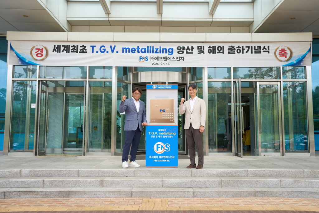
▲(왼쪽부터)에프앤에스전자 최병철, 신재호 대표가 유리기판 첫 출하 및 수출 기념식에서 기념촬영을 하고 있다.
TGV·메탈라이징 공정, SKC 자회사 앱솔릭스 공급
고성능 반도체 유리기판 제조 기업 에프앤에스전자(FNS전자, 대표 최병철, 신재호)가 반도체 유리기판 양산 후 수출하며, 유리기판 글로벌 선도에 본격 나섰다.
에프앤에스전자는 양산된 유리기판을 16일 첫 출하해 앱솔릭스(Absolics)에 수출한다고 16일 밝혔다.
에프앤에스전자는 16일 인천 송도 본사에서 최병철, 신재호 대표와 오준록 앱솔릭스 대표가 참석한 가운데 첫 출하 및 수출 기념식을 진행했다.
에프앤에스전자는 독자적인 공정 기술을 적용한 유리기판을 미국 조지아주 코빙턴에 위치한 앱솔릭스 공장에 납품한다.
앱솔릭스는 SKC가 고성능 컴퓨팅용 반도체 유리기판 사업을 위해 2021년 설립한 자회사다.
에프앤에스전자는 올해 세계 최초로 글라스관통전극(TGV), 금속층을 형성하는 메탈라이징(metalizing) 기술이 적용된 반도체 유리기판 양산에 성공한 데 이어 첫 대량 수출의 길을 텄다.
유리기판은 반도체 칩과 메인보드를 직접 연결할 수 있는 혁신적인 기판 소재다. 표면이 매끄럽고 대형 사각형 패널로의 가공성이 우수해 초미세 선폭 반도체 패키징 구현에 적합하다.
또한 중간 기판(실리콘 인터포저)이 필요 없어 기판 두께를 25% 줄일 수 있고, 패키징 영역에서 사용되는 다른 소재에 비해 소비 전력을 30% 이상 줄일 수 있다.
2021년 설립된 에프앤에스전자는 같은 해 경북 구미에 연구개발(R&D)센터를 마련하고 유리기판 제조 핵심 기술 개발을 통해 글로벌 수준의 경쟁력을 확보해왔다. 올해 반도체 유리기판 양산에 성공하며 높은 기술력과 생산 능력을 인정받았다. 에프앤에스전자 유리기판 공장은 송도에 위치하며, 양산 공장에서의 수율 개선을 통한 대량 생산 체계를 위해 장비 및 인력이 추가 투입될 예정이다.
에프앤에스전자는 최근 첨단 기술력과 뛰어난 양산 능력을 높게 평가받아 다양한 투자사로부터 대규모 투자를 유치했다. 투자 금액은 우수한 인력 및 장비 확충, 기술 개발, 글로벌 시장 진출 확대를 위해 사용된다.
TGV는 유리기판에 미세한 구멍(홀)을 뚫어 전기적 신호를 전달하는 기술로 유리기판 양산 공정의 핵심이다. 메탈라이징은 기판에 금속 박막을 형성하는 공정으로 높은 순도와 밀도를 통해 우수한 접착력을 제공한다. TGV, 메탈라이징 공정이 적용된 유리기판을 제조하는 기업은 현재 에프앤에스전자가 전 세계 유일하다.
최병철 에프앤에스전자 대표이사는 “유리기판은 반도체 패키징 분야의 판도를 바꿀 혁신적 기술로 글로벌 반도체 기업 대부분이 도입을 검토 중”이라며 “이번 첫 수출은 에프앤에스전자의 유리기판 핵심 공정 기술 역량을 인정받은 성과로 향후 글로벌 시장 공략의 중요한 발판으로 평가된다. 앞으로 국내외 고객을 지속적으로 확보하며 전 세계 유리기판 시장을 선도해 나갈 것”이라고 밝혔다.
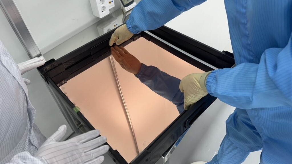
▲에프앤에스전자가 양산 및 첫 수출한 반도체 유리기판