한국전자통신연구원(ETRI)이 텔레륨(Te) 기반의 칼코지나이드계 p형 반도체 소재를 활용해 상온증착이 가능하면서도 공정이 단순한 p형 Se-Te(셀레늄-텔레늄) 합금 트랜지스터를 개발하며, 향후 차세대 디스플레이 및 초저전력 반도체 소자 성능개선에 널리 활용될 전망이다.
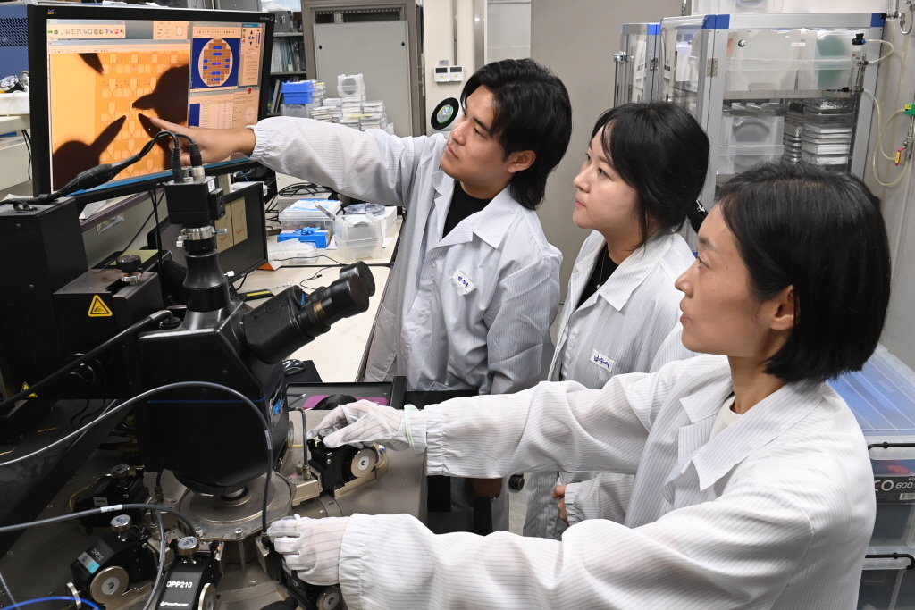
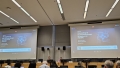
▲ETRI researchers measuring the electrical characteristics of a p-type semiconductor device while looking at its image.
Overcoming low mobility of p-type semiconductors, improving display refresh rate and power consumption
Overcoming the limitations of semiconductor microprocessing, a new paradigm for stacked semiconductors is expected
The Electronics and Telecommunications Research Institute (ETRI) has succeeded in developing p-type semiconductor materials and thin-film transistors utilizing them, which will lead innovation in the semiconductor industry. It is expected to be widely used in improving the performance of next-generation displays and ultra-low-power semiconductor devices in the future.
ETRI announced on the 23rd that it has developed a p-type Se-Te (selenium-tellurium) alloy transistor that can be deposited at room temperature and has a simple process using a chalcogenide p-type semiconductor material based on tellurium (Te).
In addition, a technology was developed that can systematically control the threshold voltage of an n-type transistor by controlling charge injection into a Te thin film in a heterojunction structure of an n-type oxide semiconductor and a p-type Te.
These results were published in the world-renowned academic journal 'American Chemical Society (ACS) Applied Materials and Interfaces' in April and last month, respectively.
Semiconductors are divided into intrinsic semiconductors and impurity semiconductors depending on whether they are doped or not.
A genuine semiconductor is a semiconductor in its pure state without any impurities added.
In the case of silicon, which is commonly used in semiconductors, pure silicon does not allow electrons to move, so no current flows even if voltage is applied.
Therefore, by adding specific impurities to the genuine semiconductor, the characteristics and electrical conductivity of the semiconductor are adjusted and utilized.
Impurity semiconductors are classified into n-type semiconductors and p-type semiconductors depending on the added impurities.
The material widely used in the current display field is mainly n-type oxide semiconductor based on indium gallium zinc oxide (IGZO).
In the case of p-type oxide semiconductors, electrical characteristics and processability are not secured compared to n-type oxide semiconductors, so p-type low-temperature polycrystalline silicon (LTPS) is used, but there are limitations in that manufacturing costs are high and there are restrictions on the substrate size.
On the other hand, interest in the development of p-type semiconductors is increasing as a refresh rate of 240 Hz or higher is required for recent high-resolution displays, especially SHV-class (8K*4K) resolutions.
br /> Since there are limitations in implementing displays with high refresh rates using only n-type semiconductor-based transistors used in existing displays, demand for p-type semiconductors with characteristics comparable to n-type is increasing.
Accordingly, the ETRI research team succeeded in developing a p-type semiconductor by adding Se to Te to increase the crystallization temperature of the channel layer, depositing an amorphous thin film at room temperature, and then crystallizing it through subsequent heat treatment.
As a result, improved mobility and higher on-offline current ratio characteristics compared to existing transistors were secured.
The research team also confirmed that when a Te-based p-type semiconductor was introduced as a heterojunction structure on top of an n-type oxide semiconductor thin film, the threshold voltage of the n-type transistor could be adjusted by controlling the flow of electrons in the n-type transistor depending on the thickness of Te.
In particular, the stability of n-type transistors was improved by controlling the thickness of Te in a heterojunction structure without a passivation layer.
By utilizing this achievement, the development of the next-generation display industry that satisfies both high resolution and low power consumption is expected to accelerate.
This achievement has excellent applicability not only in the display industry but also in the semiconductor industry.
Currently, the world's leading semiconductor companies are developing fine processes to increase the integration of semiconductors, but many experts are analyzing that the increase in semiconductor integration has reached its limit.
Recently, a stacking method that stacks multiple semiconductor chips is being utilized.
Through-silicon via (TSV) is the most representative stacking method, which stacks multiple wafers and electrically connects them by drilling holes.
This has the advantage of increasing space utilization on the substrate and reducing power consumption.
On the other hand, there are many problems to overcome, such as high process costs and low yields.br />
To overcome the limitations of TSV, the monolithic 3D (M3D) method, which stacks materials layer by layer on a single wafer instead of stacking multiple wafers, has recently been in the spotlight.
On the other hand, it has not yet reached the commercialization stage due to limitations such as limited use of high-temperature processes.
Meanwhile, the n-type oxide semiconductor and Te-based p-type semiconductor heterojunction thin film transistor and p-type semiconductor device developed by the ETRI research team are evaluated to have brought one step closer to commercialization of M3D by operating stably even in a process below 300℃.
ETRI Flexible Electronics Research Lab Principal Researcher Seong-Haeng Cho said, “This is an important achievement that can be widely used in the next-generation display field, such as OLED TV and extended reality (XR) devices, as well as ultra-low-power complementary metal-oxide semiconductor (CMOS) circuits and DRAM memory research.”
The ETRI research team announced that they plan to optimize Te-based p-type semiconductors on large-area substrates of 6 inches or larger, apply them to various circuits, secure commercialization potential, and then apply them to various application fields.
This research was conducted as a project of the National Research Council of Science and Technology's Creative Convergence Research Project, 'Development of Ultra-low Power Consumption, High Bandwidth, Large-Capacity DRAM Based on M3D Oxide Semiconductor', 'Development of Core Technology for Non-silicon Semiconductor TFT Capable of High-Resolution, Large-Area Display and CMOS Manufacturing Utilizing It' of the Ministry of Trade, Industry and Energy's Industrial Technology Challenge Track, and 'Development of High-Performance Semiconductor Transistor for Ultra-low Power Multi-Array Device' of the ETRI Next-Generation Leading Researcher Project.