기사입력 2024.12.20 10:46
본지는 머크의 기자간담회 후 아난드 남비어(Anand Nambiar) CCO를 만나 반도체와 소재 시장의 전망에 대해 들어보았다.
2024-02-05 오후 2:45:27by 성유창 기자
.jpg)
한국머크(대표이사 김우규 박사)의 자회사 중 하나인 엠케미칼㈜이 4월1일 자로 한국머크 반도체 비즈니스 법인 중 하나인 버슘머티리얼즈코리아㈜로 통합된다.
2024-04-01 오전 10:14:01by 성유창 기자
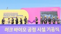
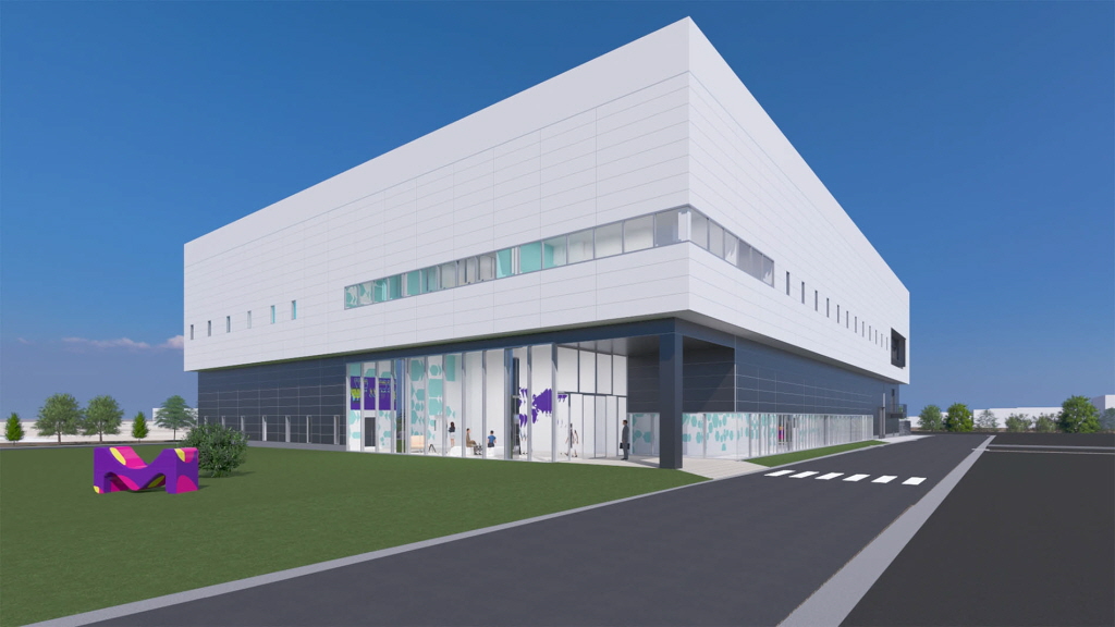
머크(Merck)가 우리나라에 바이오 산업 핵심 원부자재 아시아태평양 생산거점 구축에 4,300억원을 투자했다.
2024-05-30 오전 10:39:50by 배종인 기자
머크(Merck)가 유니티SC(Unity-SC)를 인수하며 반도체 산업에서의 과학 및 기술 기반 포트폴리오 보완 및 인공지능으로 창출된 성장 기회를 활용하는 능력을 강화한다.
2024-07-23 오전 11:04:58by 성유창 기자
디스플레이 기술은 데이터와 사용자 간의 커뮤니케이션 매개체로서 정보를 빛으로 구현하며 디바이스에 필수적인 기술로 자리매김했다. 이러한 빛의 기술에 혁신을 이끄는 머크의 재료 솔루션들이 대거 공개되며 눈길을 끌었다.
2024-08-14 오후 2:37:19by 권신혁 기자
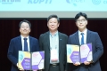
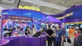
선도적인 과학기술기업 머크의 한국법인, 한국머크(대표이사 김우규 박사)는 8월20일∼23일까지 제주 국제 컨벤션센터에서 ‘Share Display, Share Life’ 주제로 열리는 ‘국제정보디스플레이학회(International meeting on Information display) 2024(이하 IMID 2024)’에 참여했다. 이번 행사에서 2024년 영예의 머크 어워드 수상자로 박진성 한양대학교 교수가 선정됐다. 젊은 과학자 상은 정승준 고려대학교 교수가 수상의 영예를 안았다.
2024-08-22 오전 8:21:34by 배종인 기자
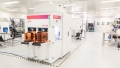
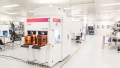
선도적인 과학기술기업 머크의 한국법인인, 한국머크(대표이사 김우규 박사, Merck)가 경기도 안성에 한국 SOD 어플리케이션 센터(KSAC)를 개소하고, 고대역폭 메모리, 첨단 로직 칩 개발에 매우 중요한 스핀온 절연막(SOD, Spin on Dielectric)의 한국 현지 공급 능력을 갖췄다.
2024-10-10 오후 5:09:00by 배종인 기자
선도적인 과학기술기업인 머크의 한국지사(대표이사 김우규 박사)가 반도체 검사 장비 업체인 유니티SC 인수를 완료하며, 유니티SC의 검사 역량을 활용한 광전자공학 분야의 신제품 개발로 기존 디스플레이 사업부 내 광학 기술 역량이 강화될 것으로 기대된다.
2024-11-06 오전 9:44:57by 배종인 기자

[열린보도원칙] 당 매체는 독자와 취재원 등 뉴스이용자의 권리 보장을 위해 반론이나 정정보도, 추후보도를 요청할 수 있는 창구를 열어두고 있음을 알려드립니다.
고충처리인 장은성 070-4699-5321 , news@e4ds.com