글로벌 종합 반도체 연구개발 기관 Imec의 루크 반 덴 호브 CEO가 차세대 반도체 기술 발전을 위한 협력을 강조하며, 5~10년을 내다보는 미래 반도체 기술 개발의 비전을 공개했다. 루크 반 덴 호브 CEO는 “나노시트가 3세대 이후로는 CFET 기술이 적용될 것으로 본다”라고 전망했다.
.jpg)
▲루크 반 덴 호브 Imec CEO
Imec 기자간담회 개최, 반도체 글로벌 생태계 강조
의료·제약 산업 반도체 혁신 기대...DNA 시퀀싱 가속
국내 최대 반도체 장비·소재 전시회 세미콘 2025 개최를 앞두고 글로벌 반도체 관련 기업들이 앞다퉈 한국을 방문했다.
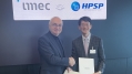
글로벌 종합 반도체 연구개발 기관 Imec이 18일 서울 삼성동 그랜드 인터컨티넨탈 서울 파르나스에서 기자간담회를 개최했다.
Imec 연구 분야와 주요 성과를 발표한 이번 간담회에서는 루크 반 덴 호브 imec CEO가 차세대 반도체 기술 발전을 위한 협력을 강조하며, 5~10년을 내다보는 미래 반도체 기술 개발의 비전을 공개했다.
루크 반 덴 호브 CEO는 “Imec은 산업제휴모델을 도입해 인텔, TI, 삼성전자, TSMC 등 주요 기업들과 선행 연구 협력해왔다”면서, “300mm 웨이퍼 전환과 핵심 CMOS 프로그램 출범시켜 주요 반도체 기업들을 유치했다”고 강조했다.
Imec은 지정학적 위기 속에서도 반도체 혁신을 위한 글로벌 협업이 무엇보다고 중요하다고 강조하며, Imec이 개발하는 5~10년을 내다보는 차세대 기술들을 소개했다.
Imec은 정밀해지는 웨이퍼 본딩 기술을 활용해 백사이드 인터커넥트 로드맵을 도입하고 있으며, n-채널과 p-채널 소자를 적층하는 나노시트 컨셉을 확장해 리소그래피 기반 방식 이상의 스케일링 실현을 도모하고 있다.
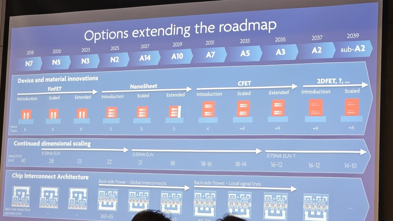
▲Imec 반도체 기술 로드맵
반 덴 호브 CEO는 “패키징 기술의 중요성도 높아져 집적도를 높이는 어드밴스드 패키징이 이종 칩간 인터커넥트 속도를 높여줘 AI 시대 성능 향상에 큰 담당을 하고 있다”고 평가하면서, “나노시트가 3세대 이후로는 CFET 기술이 적용될 것으로 본다”라고 전망했다.
CFET은 GAA 구조의 트랜지스터를 수직으로 쌓아 올리는 구조로 트랜지스터 집적도를 높이고 면적을 줄일 수 있어 반도체 효율을 극대화할 수 있는 차세대 소자 구조로 연구되고 있다. 이러한 CFET을 Imec이 연구하며 차세대 소자 출현을 예고하고 있다.
또한 Imec은 의료 및 제약 산업에서의 반도체 혁신을 기대하고 있었다. Imec은 반도체 기술을 이용해 DNA 시퀀싱을 가속화하고 있으며, 이를 위한 포토닉스, 이미징 기술, 미세유체공학 등을 반도체에 통합하고 있다.
이러한 나노전자 기술 기반으로 Imec은 뉴로픽셀 프로브를 개발했으며, 뉴로픽셀 2.0은 5,000개 이상의 기록 지점을 작은 뇌 임플란트에 탑재해 뇌 영역과 회로에서 뉴런 기록을 가능하게 한다. 이를 통한 뇌 연구와 이해도 혁신을 기대했다.
루크 반 덴 호브 CEO는 트럼프 2.0시대 미중갈등과 국가 간 관세전쟁과 관련해 “최근 지정학적 이슈로 위협요소가 대두되고 있지만 연구개발의 디커플링은 혁신 속도를 늦출 뿐”이라며, “기술 개발이 어려워지는 과정 속에서 산업 전반 디커플링은 심화되지 않을 것”이라고 전망했다.
한편, 같은 날 오후 개최된 Imec 테크놀로지 포럼 코리아(ITF KOREA)에서는 루크 반 덴 호브 CEO의 오프닝 기조연설을 시작으로 △삼성전자 △SK하이닉스 △ASML 등이 참여해 미래 반도체 기술의 미래에 대해 발표했다.