5G 시대에 걸맞게 PCI 익스프레스 4.0, USB 3.1, UFS, PAM4 등을 탑재한 디바이스가 늘고 있다. 이러한 디바이스는 대용량 데이터를 고속으로 처리해야 한다. 또한 디바이스의 동작 전압이 낮아지는 동시에 전류는 높아지고 있으며, PCB의 고밀도화 및 고다층화가 진행됨에 따라 엔지니어들은 설계 초기부터 면밀한 설계 및 검증을 필수적으로 수행해야 한다. ADS는 RF, 마이크로웨이브 및 신호 무결성 애플리케이션을 위한 전자 설계 자동화 소프트웨어로, 표준 기반 설계 및 검증 환경을 제공한다.
5G 시대 도래로 고속 전송 신호 구현 필수
제품 설계 단계부터 정확한 분석 필요성 증가
ADS, 협업으로 개발 키트, 부품 라이브러리 지원

지금 이 순간에도 대용량 데이터가 고속으로 처리되고 있다
5G의 상용화 시점이 점점 다가오고 있다. 머지않아 모든 사물이 인터넷으로 연결되는 시대가 열릴 것이다.
5G의 특징은 ‘초고속’, ‘저지연’, ‘초연결’이다.
먼저 5G는 전 세대보다 훨씬 빠른 초고속 이동통신이다. 5G는 사용자당 100Mbps에서 최대 20Gbps까지의 데이터를 처리하는데, LTE(4G) 대비 20배나 높은 수준이다. 또한 5G의 지연 시간은 극도로 짧다. LTE의 지연 시간은 10ms이나, 5G는 1ms로 10배나 짧다. 마지막으로 수많은 디바이스를 동시에 연결할 수 있다. LTE가 1km
2당 최대 10만 개 디바이스를 연결하는 반면, 5G는 최대 100만 개의 기기를 연결할 수 있다.
네트워크에 연결된 수많은 IoT 디바이스의 방대한 데이터를 처리하는 위해서는 고속 전송 신호의 구현이 필수적이다. 신호 무결성과 전원 무결성 확보 또한 더욱 중요해지고 있다. 지금도 다양한 전송 신호 규격이 생겨나고 있으며, 그 사양 또한 더욱 엄격해지고 있다.
위와 같은 어려움을 해결하기 위해서는 제품 설계 단계부터 정확한 분석이 필요하다.
대용량 데이터 고속 처리 디바이스 설계의 어려움
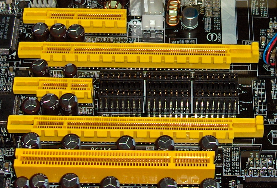
다양한 PCI 익스프레스 슬롯
5G 시대에 걸맞게 PCI 익스프레스 4.0, USB 3.1, UFS, PAM4 등을 탑재한 디바이스가 늘고 있다. 이러한 디바이스는 대용량 데이터를 고속으로 처리해야 하기 때문에 엔지니어들은 제품 설계 단계부터 여러 어려움에 직면한다.
어려움들에 대해 살펴보자면, 먼저 고주파 성분의 감쇠 현상이 심해지고 있다. 이제 엔지니어는 채널 설계에 더욱 신경을 써야 한다. 전송 거리에 따른 고주파 감쇠를 보상하기 위한 송수신 모듈의 다양한 이퀄라이저를 적절히 설정하고 해석하는 것 또한 중요해졌다.
그리고 디바이스의 동작 전압이 낮아지는 동시에 전류는 높아지고 있으며, PCB의 고밀도화 및 고다층화가 진행되고 있다. 또한, 제품 사양이 엄격해지면서 엔지니어들은 설계 초기부터 면밀한 설계 및 검증을 필수적으로 수행해야 한다. 그러나 이는 쉽지 않다.
일반적인 설계 플로를 살펴보자.
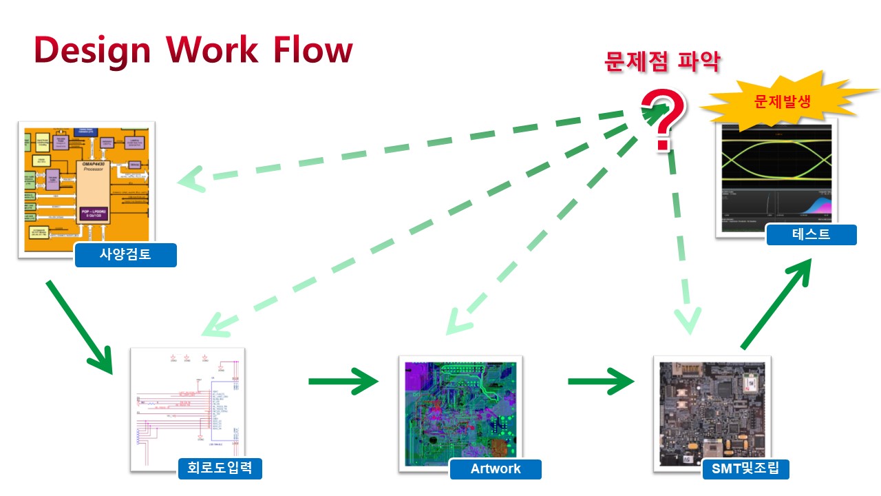
완성된 제품의 된 문제가 어디서 발생했는지 찾아내는 것은 힘든 작업이다
먼저 제품 기획 단계에서 제품 개발을 위한 사양 검토를 실시한다. 사양 검토를 마치면 회로도를 완성한다. 그리고 실제 PCB 제작을 위해 아트워크 엔지니어와 협업하여 부품을 배치하고 선로 배선을 마친다.
PCB 설계가 끝나면 완성된 거버 파일(Gerber File)을 PCB 제작업체에 보내 PCB를 제작하고, SMT 조립라인에서 부품을 마운팅 한다. 완성된 제품의 검증은 측정장비를 통해 최종적으로 확인하고 문제가 없다면 제품을 출시한다.
그런데 문제가 있다면? 문제가 어디서 발생했는지 어떻게 알 것인가? 시간과 자원이 많다면 어떻게든 알 수 있겠지만, 고단한 작업이 될 것이다. 그러나 설계 중간중간 시뮬레이션 과정을 거쳤다면?
전자 설계 자동화 소프트웨어를 이용하면 간단하게 문제를 파악할 수 있다.
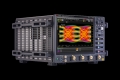
키사이트의 전자 설계 자동화 소프트웨어, ADS란?
키사이트 ADS 실행 화면
키사이트 ADS는 RF, 마이크로웨이브 및 신호 무결성 애플리케이션을 위한 전자 설계 자동화 소프트웨어다. e4ds.com에서 진행한 관련 웨비나에 의하면, ADS는 회로 시뮬레이터로서, 포인트 툴 솔루션이 아닌 결합적인 워크 플로의 역할을 수행한다.
와이맥스, LTE, 멀티 기가비트 데이터 링크, 레이더 및 위성 애플리케이션을 지원하는 ADS는 통합 플랫폼에서 디자인 라이브러리 및 회로-시스템-EM 공동 시뮬레이션을 제공하는 등 표준 기반 설계 및 검증 환경을 제공한다.
ADS는 주요 부품 산업 및 파운드리 파트너와의 협업을 통해 제품 개발 키트 및 부품 라이브러리를 지원하고 있다.
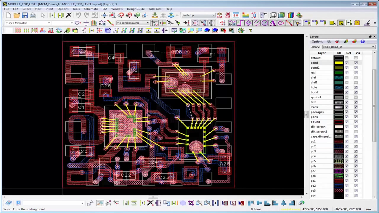
회로도 완성 후 ADS의 여러 채널 모델을 이용하여 프리 레이아웃 분석을 하면 설계하는 제품의 아트워크 설계 가이드를 제시할 수 있다. 아트워크 과정을 마친 후 포스트 레이아웃 분석에서 현재의 디자인을 한 번 더 검증하는 절차를 거친다.
이 과정에서 채널들은 EM 모델로 추출하게 되고, 시간축에서의 TDR이나 트랜션트 해석을 통해 신호 품질을 확인할 수 있다. 이렇게 두 차례 사전 검증 과정을 거치면 실제 테스트 과정에서 발생하는 신호 무결성이나 전원 무결성 등의 문제들을 미리 줄일 수 있다.
시뮬레이션으로 레이아웃 명확히 검증하기

PCB 전송선로 검증은 정확한 사전분석이 필요하다
시뮬레이션을 설계 워크 플로에 적용하면 레이아웃을 명확하게 검증할 수 있다.
추상적인 제품 구상 단계에서 실제 모델의 구체적인 단계에 도달하기 위해서는 레이아웃에 대한 명확한 검증이 필요하다. 특히 PCB 대부분을 구성하고 있는 전송선로의 검증은 분명한 모델을 통한 정확한 사전분석이 필요하다.
포스트 레이아웃 단계에서는 PCB에 존재하는 다양한 기생 성분과 더불어 전자계 기반 모델 추출 및 검증을 통해 추가로 신호 무결성이나 전원 무결성을 확인해야 한다.
마지막 테스트 단계인 규격 테스트 과정에서 Eye Open에 문제가 있는 경우 어떤 식으로 문제를 해결해야 할까?
부품이 문제인 경우 다른 샘플과의 비교를 통해 문제점을 찾을 수 있다. 회로도 입력 오류나 코딩 에러는 많은 시간을 들여서 해결해야 한다.
신호 무결성, 전원 무결성 문제는 시뮬레이션을 통해서 검증을 하는 것이 효과적이다.
간단한 예제를 통해 살펴보자.
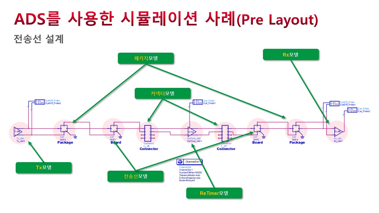
ADS의 IBIS AMI 모델 사용 시뮬레이션 사례
이미지는 키사이트 시뮬레이션 환경인 ADS의 IBIS AMI 모델을 사용한 시뮬레이션 사례다.
ADS schematic에는 여러 채널 모델들이 구성되어 있다. 패키지 모델, 전송선 모델, 커넥터 모델, 그리고 IBIS AMI 모델을 이용하여 이미지와 같은 회로를 구성하였다.
채널을 완성하고 실제 시뮬레이션을 수행하게 되면 이미지와 같이 단계별로 신호 품질 수준을 확인할 수 있다.
시뮬레이션의 장점은 미리 다양한 경우의 수를 검증할 수 있다는 것이다.
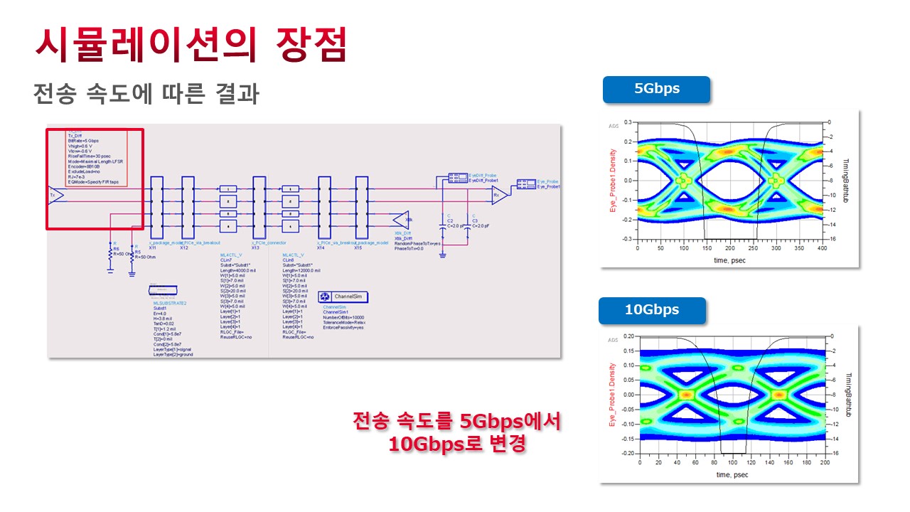
전송 속도에 따른 채널 마진 확인하기
다음과 같이 Tx의 전송 속도를 변경할 경우 채널이 어느 정도 마진을 가지고 있는지 확인할 수 있다. 그뿐만 아니라 아직 설계되지 않은 PCB의 선폭이나 선로 간 간격을 시뮬레이션 하여 최적을 설계값을 찾는 것도 쉽다.
Tx 모델로 많이 사용되고 있는 IBIS AMI Model의 경우 모델 특화적인 내용이 많다. 그 예로 Tx의 emphasis 탭 수를 조절하는 경우다. 개발자는 ADS를 통해 사전에 여러 경우의 수 결과들을 확인할 수 있다.
전송 신호의 공급원인 Tx 디바이스, Rx 디바이스의 모델들은 IBIS AMI 파일 형태로 업체로부터 공급받고 있다. 예를 들어 PCI 익스프레스 신호를 전송하는 칩셋을 엔지니어가 사용하고 있다면 해당 칩셋 제조사로부터 파일을 요청할 수 있다. 하지만 칩셋 제조사의 사정에 따라 IBIS 모델 혹은 SPICE 모델 형태로 공급받을 수도 있다. IBIS AMI 모델의 경우 칩셋 내부의 이퀄라이저 같은 디지털 부분을 dll 파일로 암호화한 모델이기 때문에 SerDes 애플리케이션에 적합하다.
신호들이 통과하는 채널들, 즉 패키지나 PCB 전송선로들은 S-파라미터라 불리는 모델로 모델링 된다. 채널 모델의 경우 업체로부터 제공을 받거나, 커넥터 모델의 S-파라미터를 받는 것뿐만 아니라 엔지니어가 스스로 생성하기도 한다.
해당 모델을 정확하게 얻기 위해선 측정 또는 EM 해석을 통해 모델링 하게 된다. 측정 모델의 경우 계측장비의 대역폭 설정이나 측정 셋업 조건을 유의해야 하며 EM 해석 기반 모델링을 할 경우에는 포트 셋업과 같은 해석 조건 설정을 정확히 하는 것이 관건이다.
e4ds.com에서 10월 4일 진행한 관련 웨비나에서는 설계가 끝난 PCB를 ADS 환경으로 불러와 전자계 해석을 하고, S-파라미터 모델을 생성하여 분석하는 과정에 대해 추가적으로 다뤘다. 또한, ADS 신호 무결성 전자계 해석 툴인 SIPro를 활용한 EM 해석 등의 데모도 선보였다. 해당 웨비나는 다시보기가 가능하다.
각 분야의 엔지니어들은 ADS 웨비나를 보면서 Q&A 란을 통해 다양한 질문을 쏟아냈다.
먼저 ADS의 적용 및 응용범위에 대해 묻는 질문이었다; ADS는 다양한 분야에서 활용할 수 있다. RFuW, 고속 디지털, 디바이스 모델링, ESL, RFIC 등 IC부터 전체 시스템에 대한 적용이 가능하다.
또한 ADS가 내보내기 가능한 거버 파일의 종류에 대해 묻는 질문이었다; ADS가 내보낼 수 있는 거버 파일은 ODB++, .brd 파일 외 다수다.
마지막으로 ADS를 활용한 작업 방식과 기존 작업 방식의 차이점에 대해 묻는 질문이었다; 기존 작업 방식은 시도 횟수와 에러가 많을 수밖에 없었다. 하지만 ADS와 같은 자동화 시뮬레이션 프로그램은 이미 만들어져 있는 디자인 가이드를 적용하여 보다 빠르게 제품을 검증할 수 있다.