재료연, 반도체 장비 내부 오염 줄인다
기사입력 2023.03.22 16:14
내플라즈마성 세라믹 나노복합체 신조성·공정 기술
반도체 장비 내부의 오염 입자를 줄이는 기술이 개발돼 향후 세라믹 부품의 교체 주기가 길어질 것으로 기대된다.
과학기술정보통신부 산하 정부출연연구기관인 한국재료연구원(KIMS, 원장 이정환)은 최근 엔지니어링세라믹연구실 마호진, 박영조 박사 연구팀이 반도체 제조 장비 내부의 오염 입자를 줄이는 내플라즈마성 세라믹 나노복합체 신조성 및 공정 기술을 국내 최초로 개발하는 데 성공했다고 22일 밝혔다.
일반적인 반도체 공정은 플라즈마를 이용한 식각 공정으로 이뤄진다.
이 과정에서 실리콘 웨이퍼는 물론, 장비의 내부 부품까지 플라즈마에 노출돼 오염 입자를 생성하여 칩 불량이 발생하는 일이 빈번하다.
이로 인해 장비 내부 소재의 90% 이상을 차지하는 세라믹 부품의 잦은 교체는 반도체 생산성을 저해하는 큰 원인이 되기도 한다.
연구팀은 기존의 단일 조성 세라믹이 아닌 나노복합체를 이용해 이트리아-마그네시아(Y2O3-MgO) 소재를 10나노미터(㎚) 크기의 입자로 합성하고, 무기공 치밀체 소결 공정 기술을 통해 100% 밀도의 완전 치밀체를 제작했다.
식각율이 작을수록 우수한 소재인데, 개발된 나노복합체는 사파이어와 비교하면 6.5%, 플라즈마 저항성이 가장 우수하다고 알려진 이트리아(Y2O3)와 비교해서도 40% 정도에 불과했다.
이외에도 연구팀은 나노복합체의 미세구조 내 결정립 크기와 기공도에 따라 플라즈마 식각 후에 나타나는 표면 변화를 분석하고, 미세하고 균일한 미세구조 분포를 가진 나노복합체가 우수한 식각 저항성과 적은 표면 조도 변화를 가져온다는 사실을 확인했다.
재료연 마호진 선임연구원은 “반도체 전 공정 중 식각 공정은 미국과 일본의 장비·부품이 90% 이상을 장악하고 있으며 이를 중국이 빠르게 추격하는 추세”라며 “이번 연구성과는 세계 최고 수준의 내플라즈마성 소재를 국내 기술로 개발한 대표적 사례임과 동시에, 소재 자립화를 통해 부품을 국산화하는 초석이 될 것으로 기대한다”고 말했다.
이번 연구성과는 과학기술정보통신부의 ‘나노 및 소재기술 개발사업(국가핵심소재연구단)’의 지원을 받아 진행됐으며, 재료연은 본 기술을 ㈜맥테크(대표이사 김병학)에 기술이전 했다.
한편 해당 연구 결과는 한국표준과학연구원 이효창 박사 연구팀과 공동연구를 통해, 미국 화학회(ACS)가 발행하는 국제학술지 ‘에이씨에스 어플라이드 머티리얼즈 앤 인터페이스(ACS Applied Materials & Interfaces, IF: 10.383)에 2022년 9월22일자로 게재됐다.
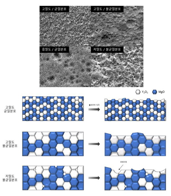
▲신조성 나노복합체 세라믹의 미세구조에 따른 플라즈마 식각 특성

관련뉴스
-
재료연·대한항공, 항공기 소재 개발 ‘맞손’
과학기술정보통신부 산하 정부출연연구기관인 한국재료연구원(KIMS, 원장 이정환)이 국내 대표 항공사인 대한항공과 손잡고 항공기 소재 부품 분야 개발에 박차를 가하기로 약속했다.
2023-02-24 오후 3:17:49by 배종인 기자
-
재료硏, KIMS 인공지능 과학토크 공모전
한국재료연구원(KIMS, 원장 이정환)이 생성형 인공지능(AI) 챗GPT 열풍을 계기로, 대화형 인공지능 플랫폼과 재료과학을 연계한 ‘KIMS 인공지능 과학토크 공모전’을 개최한다.
2023-03-02 오전 9:06:48by 배종인 기자
-
.jpg)
재료연, ‘종합서비스 기업지원사업’ 429억 매출 달성
과학기술정보통신부 산하 정부출연연구기관인 한국재료연구원(KIMS, 원장 이정환)이 기업 사업화 지원에 총력을 기울인 결과 429억원의 매출과 40명의 신규 고용 등 큰 성과를 이룬 것으로 나타났다.
2023-03-17 오후 3:20:30by 배종인 기자


많이 본 뉴스
[열린보도원칙] 당 매체는 독자와 취재원 등 뉴스이용자의 권리 보장을 위해 반론이나 정정보도, 추후보도를 요청할 수 있는 창구를 열어두고 있음을 알려드립니다.
고충처리인 장은성 070-4699-5321 , news@e4ds.com