기초과학연구원(IBS, 원장 노도영) 나노입자 연구단 김대형 부연구단장(서울대 화학생물공학부 교수)과 이상규 책임연구원 연구팀은 김지훈 부산대 교수팀과 공동으로 무손상 건식 전사 기술을 개발해 향후 독성 물질 사용을 줄이고, 소자 손상을 피할 수 있을 것으로 기대된다.
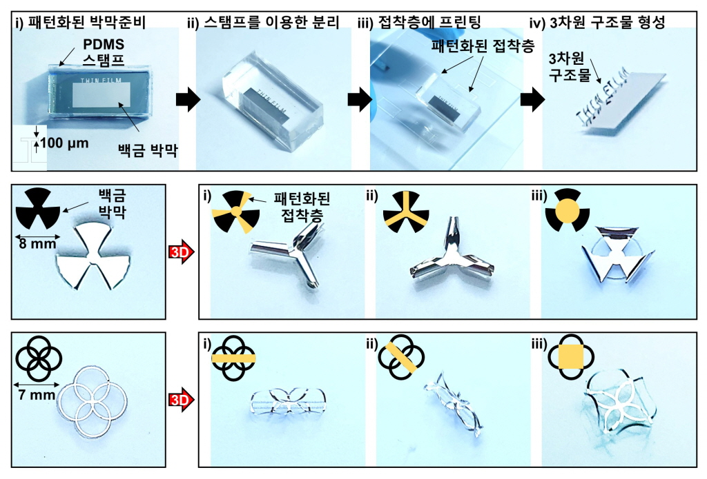
▲다양한 2차원 박막의 3차원 구조로의 변환
IBS, ‘무손상 건식 전사’ 방법 개발
스티커를 떼어내듯 고성능 전자 소자를 기판에서 손상 없이 분리하는 새로운 전사 기술이 개발됐다.
기초과학연구원(IBS, 원장 노도영) 나노입자 연구단 김대형 부연구단장(서울대 화학생물공학부 교수)과 이상규 책임연구원 연구팀은 김지훈 부산대 교수팀과 공동으로 무손상 건식 전사 기술을 개발했다고 25일 밝혔다.
전사에 필요한 시간과 비용을 대폭 줄일 수 있어 고성능 전자기기 제작에 널리 응용될 것으로 기대된다.
고성능 소자는 주로 고온에서도 안정적으로 작동하는 딱딱한 기판에서 제작된다. 유연 전자기기를 만들려면 딱딱한 기판 위의 소자를 분리해 유연한 기판으로 옮기는 전사 공정이 필수다.
기존 전사 공정은 기판과 소자 사이에 존재하는 층(희생층)을 화학물질을 이용해 제거하는 방식이었다.
강력하고 유독한 화학물질을 사용하기 때문에 작업자나 환경에 좋지 않고, 소자 손상을 피하기도 어려웠다.
이를 해결하기 위해 물에서 소자를 떼어내거나 레이저·열을 이용하는 방법 등이 개발됐지만, 여전히 고가의 장비나 별도의 후처리가 필요하고 특정 환경에서만 적용 가능하다는 한계가 있었다.
IBS 연구진은 기판 자체의 물성을 제어해 습식 화학물질이나 소자 손상 없이 소자를 손쉽게 떼어낼 수 있는 ‘무손상 건식 전사’ 방법을 개발했다.
우선 연구진은 서로 다른 응력(외력을 가할 때 변형된 물체 내부에서 발생하는 힘)을 가진 박막을 두 층으로 쌓아 올린 기판을 제작했다.
그 후 기판을 구부려 박막의 변형 에너지 방출률 변형 에너지 방출률을 최대화했다. 변형 에너지 방출률이 소자와 기판 사이의 계면 강도를 초과하면 박리가 쉽게 일어난다.
이렇게 제작한 기판 위에 소자를 제작한 뒤 스탬프(도장)를 찍고, 기판을 구부리며 스탬프를 들어 올리면 소자가 기판으로부터 간단히 분리된다. 떼어낸 소자를 원하는 기판에 옮기면 전사가 완료된다.
공동 제1저자인 신윤수 선임연구원은 “우리 연구진이 제시한 전사 방법은 독성 물질을 사용하지 않으며, 소자 손상이 적고 후처리도 필요 없어 전사 시간이 짧다는 장점이 있다”며 “대면적은 물론 마이크로 규모의 작은 패턴까지 전사가 가능해 활용 가능성이 크다”고 설명했다.
또한 연구진은 다양한 패턴의 2차원 박막을 3차원 구조체로 변형시킬 수 있음을 보여줬다. 떼어낸 소자를 옮겨 붙일 기판의 접착층 패턴에 따라 3차원 구조로 바뀔 수 있는데, 이를 이용하면 필요에 따라 다양한 구조로 만들 수 있다.
공동교신저자인 이상규 박사는 “기존 연구들과 달리 재료의 물성만을 제어하여 무손상 건식 전사 프린팅 기술을 개발했다는 것이 이번 연구의 핵심”이라며 “2차원 박막을 3차원 구조체로 변형시킬 수 있는 특징을 활용해 입체 구조를 갖는 다양한 소자 제조에 관한 후속 연구를 진행할 계획”이라고 말했다.
연구를 이끈 김대형 부연구단장은 “전사 기술은 연성 전자, 광전자, 바이오 전자 및 에너지 소자를 포함한 많은 분야에 적용된다”며 “무손상 건식 전사 기술은 새로운 고성능 전자 소자 제작에 큰 도움이 될 것으로 기대한다”고 말했다.
연구 결과는 6월21일 세계 최고 학술지인 ‘네이처 머터리얼스(Nature Materials, IF 41.2)’온라인판에 실렸다.