






All News229 articles
ASM Participates in Semiconductor Scholarship Program for Fifth Consecutive Year…Supporting Science and Engineering Talent
ASM, a semiconductor deposition equipment specialist, participated in the "21st Semiconductor Scholarship Certificate Presentation Ceremony" organized…
2026.10.23 by 배종인 기자
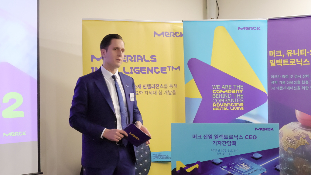
Benjamin Hein, Merck Electronics CEO: "AI is a systems battle, moving beyond materials to integrated workflow"
Benjamin Hein, CEO of Merck Electronics, stated that in the AI era, semiconductor competitiveness depends on system-wide optimization rather than indi…
2026.10.22 by 배종인 기자
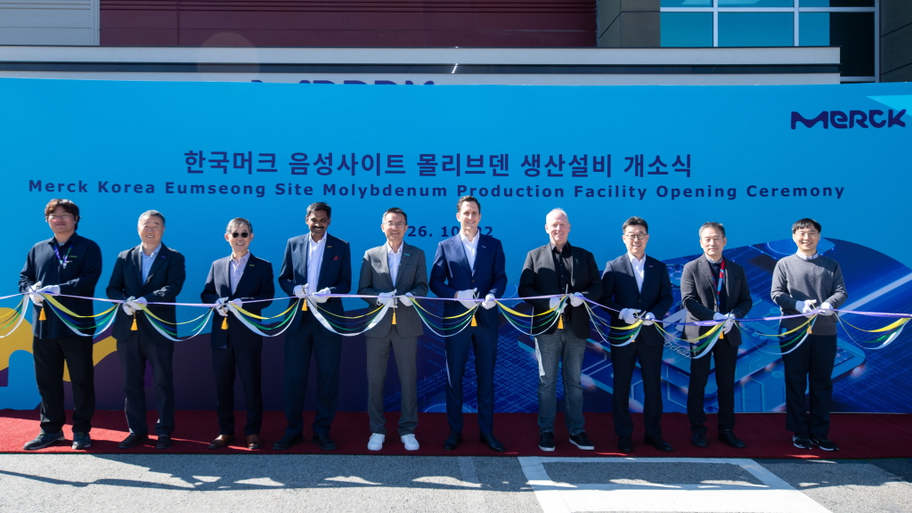
Merck Supports Next-Generation Semiconductor Innovation with Advanced Materials and Supply Technology…Opens Molybdenum Production Facility in Eumseong
Merck has established molybdenum precursor (MoO₂Cl₂) production equipment for next-generation semiconductors at its Eumseong business site in North Ch…
2026.10.22 by 배종인 기자
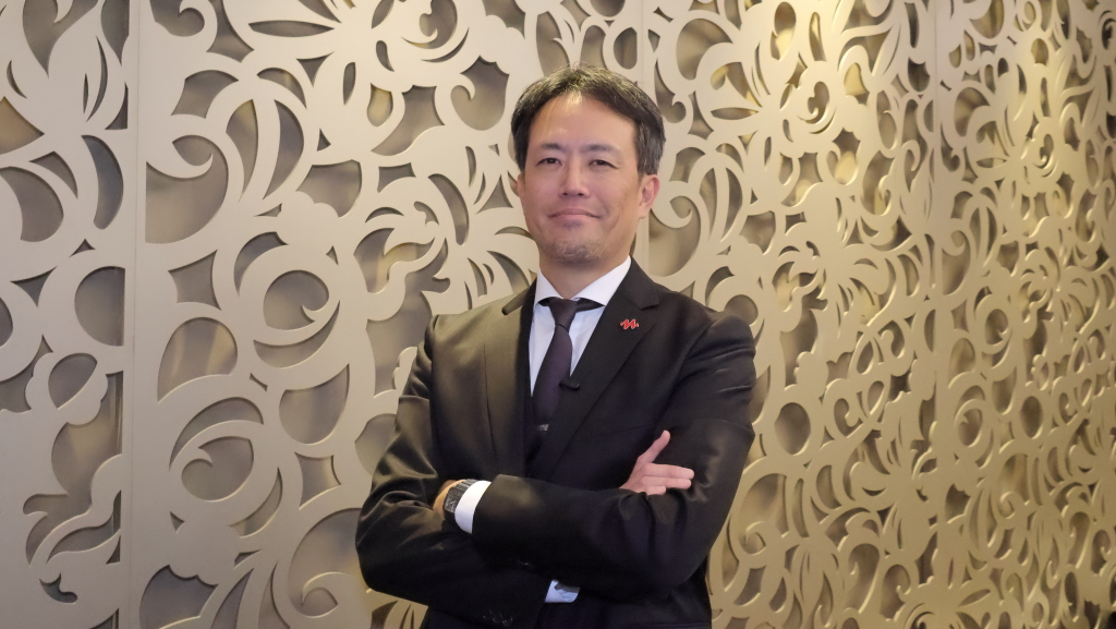
[Interview] Choi Jun-ho, Vice President of Keysight Technologies, "Supporting Advanced Technology Development Through Collaboration and Talent Behind the Frontline of Technology"
Keysight Technologies is leading technological innovation through a platform strategy that integrates design, simulation, emulation, and testing in li…
2026.10.22 by 배종인 기자
Applied Materials Korea Receives Industrial Commendation on 'Semiconductor Day'
Applied Materials Korea has received an Industrial Commendation at the 19th Semiconductor Day ceremony in recognition of its contributions to strength…
2026.10.22 by 배종인 기자
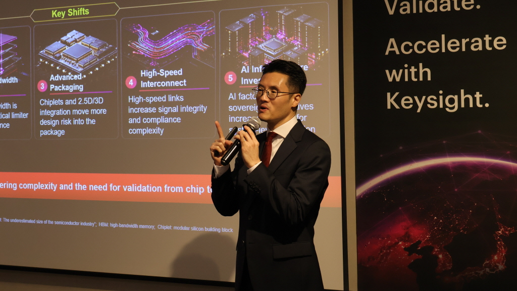
Keysight, "Evolving into an Engineering Platform Company Opening the AI Era"
Keysight Technologies held Keysight World Tech Day Seoul 2026 and shared core technologies and design and validation strategies in AI semiconductors, …
2026.10.21 by 배종인 기자
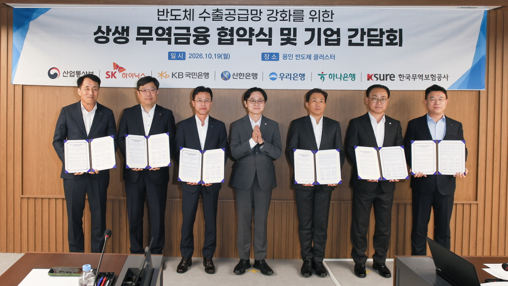
SK Hynix Launches '2 Trillion Won Export Supply Chain Strengthening Guarantee' Program for Materials, Parts, and Equipment Support
SK Hynix has launched a 2 trillion won-scale financial support program for small and medium-sized semiconductor materials, parts, and equipment compan…
2026.10.19 by 배종인 기자
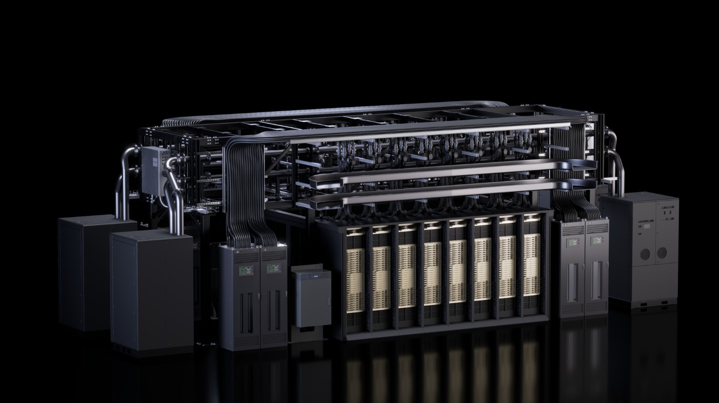

Nvidia Makes Bold Move to Become AI Datacenter 'Operating System'
At the OCP Global Summit 2026, Nvidia disclosed not only the rack design of its next-generation AI platform 'Vera Rubin,' but also extensively reveale…
2026.10.16 by 배종인 기자
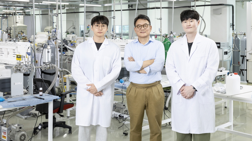
IBS Implements Semiconductor, Insulator, and Electrode in One Step through Atomic Substitution…Develops Next-Generation 2D Semiconductor Process
A research team at the Institute for Basic Science (IBS) has successfully developed a technology to selectively replace atoms in 2D semiconductors and…
2026.10.16 by 배종인 기자
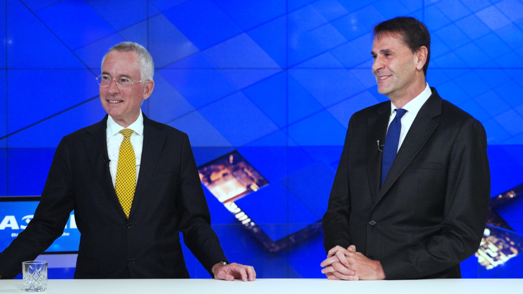
ASML records record-breaking Q3 results... "ASML production capacity determines the ceiling for advanced semiconductor supply"
ASML's Q3 2026 results demonstrate that the semiconductor industry is entering a new phase. The company achieved record-breaking results with revenue …
2026.10.16 by 배종인 기자
Xcena Demonstrates CXL-based AI Inference Memory Solution at OCP Summit
Fabless company Xcena unveiled AI inference technology utilizing CXL-based memory solution 'MX1' at OCP Global Summit 2026. In collaboration with SK H…
2026.10.16 by 배종인 기자

Arm Announces CPU Benchmarking Methodology for Agentic AI
Arm has announced a CPU performance evaluation methodology specialized for agentic AI workloads. Developed with support from Fujitsu, Meta, and OpenAI…
2026.10.15 by 배종인 기자
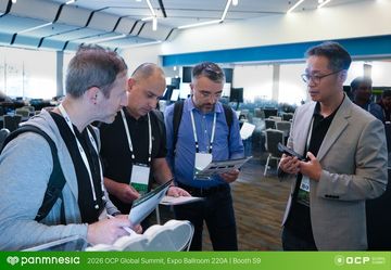
Panasia Accelerates CXL Appliance Deployment at OCP Global Summit 2026
Panasia unveiled a complete CXL server rack solution based on PCIe 6.4-CXL 3.2 fusion switch technology at OCP Global Summit 2026. As memory demand in…
2026.10.15 by 배종인 기자
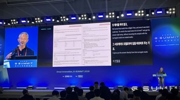
SiHighSys partners with Gyeonggi-do fabless companies at G-SUMMIT 2026
SiHighSys participated in G-SUMMIT 2026 alongside four Gyeonggi-do fabless startups, operating a joint booth, hosting presentation sessions, and organ…
2026.10.15 by 배종인 기자
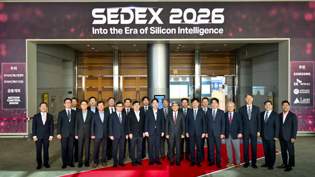
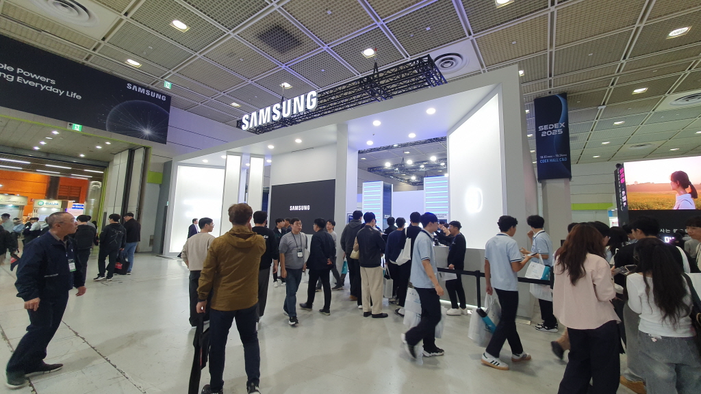
SEDEX 2026 Opens...Keynote and VIP Tour Held
The Korea Semiconductor Industry Association-organized semiconductor equipment and materials specialist exhibition 'SEDEX 2026' officially opened on t…
2026.10.14 by 배종인 기자