높은 대역폭과 빠른 데이터 속도에 대한 요구와 함께 시스템 주파수 및 변조 속도에 대한 요구 역시 계속해서 높아지고 있다. 저전력 특성도 중요해졌다. 이제 개발자는 전기적 성능이나 기능을 희생하지 않으면서 이러한 요구들을 충족해야 한다. ADI의 마이크로파 광대역 합성기인 ADF5610은 이를 위해 PLL과 VCO을 통합했다.
ADI ADF5610, 통신·계측 시스템용으로 적합
VCO 통합으로 추가 회로 및 룩업 테이블 불필요
PLL로 38fs 미만 rms 지터 수치 달성 가능해
높은 대역폭과 빠른 데이터 속도에 대한 요구와 함께, 시스템 주파수 및 변조 속도에 대한 요구 역시 계속해서 높아지고 있다. 한때 군용 또는 방산 분야에서만 사용됐던 애플리케이션들이 상용 시장에서도 사용되면서 저전력 특성도 중요해졌다.
이제 개발자는 전기적 성능이나 기능을 희생하지 않으면서 위의 요구들을 충족해야 한다. 이를 위해서는 신호 대 잡음 비(Signal-to-noise ratio; SNR), 비트 오류율(Bit error rate; BER), 서비스 품질(Quality of service; QoS) 같은 것들을 높여야 하며, 로컬 오실레이터(Local oscillator; LO)의 위상 잡음도 잡아야 한다.
아나로그디바이스(ADI)의 ADF5610은 위상 동기 루프(Phase-locked loop; PLL)와 전압 제어 오실레이터(Voltage controlled oscillator; VCO)를 통합한 마이크로파 광대역 합성기로, 위의 요구들을 충족하려는 솔루션들을 위해 제작됐다.
넓은 주파수 커버리지
ADF5610은 총 8개의 옥타브를 지원하며, VCO 기본 주파수는 3.65GHz~7.3GHz이고 이것을 PLL로 전달해서 위상 잡음을 최소화한다.
싱글 엔드 출력(RFOUT)은 기본 주파수 범위를 두 배로 해서 7.3GHz~14.6GHz를 제공하고, 차동 출력은 1/2/4/8/16/32/64/128 설정의 분주를 사용해서 57MHz~14.6GHz의 전체 동작 범위를 지원한다.
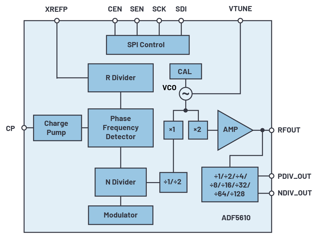
▲ ADF5610 블록 다이어그램 [그림=ADI]
ADF5610의 VCO 아키텍처는 광대역 합성기 성능을 제공할 뿐 아니라, 10GHz에서 100kHz의 오프셋에서 -114dBc/Hz 공칭 개방 루프 위상 잡음 성능을 유지한다.
내부 상태기는 수동 루프 필터만을 사용해서 40ms 미만의 주파수 안정화 시간을 달성한다. 이보다 빠른 안정화 시간이 필요하지 않다면 추가적인 회로나 룩업 테이블(Lookup table; LUT)을 사용할 필요가 없다.
컨버터 클록용으로 적합한 PLL 성능
ADF5610의 PLL은 -229dBc/Hz(고전류 모드로는 -232dBc/Hz)의 평범한 FOM(Figure of merit)을 나타내지만, 1/f 잡음(-129dBc/Hz) 및 VCO 위상 잡음 특성과 결합하면 38fs 미만의 rms 지터 수치를 달성(1kHz~100MHz 적분 한계)할 수 있다.
이는 ADF5610이 까다로운 컨버터 클록 애플리케이션에 사용하기 적합한 이유다.
열잡음과 고주파(100MHz)를 낮추기 위해서는 루프 필터 저항값을 최소한으로 유지해야 한다. 이 정도 성능 수준을 달성하려면 잡음이 극히 낮은 레퍼런스 소스가 필요하다.
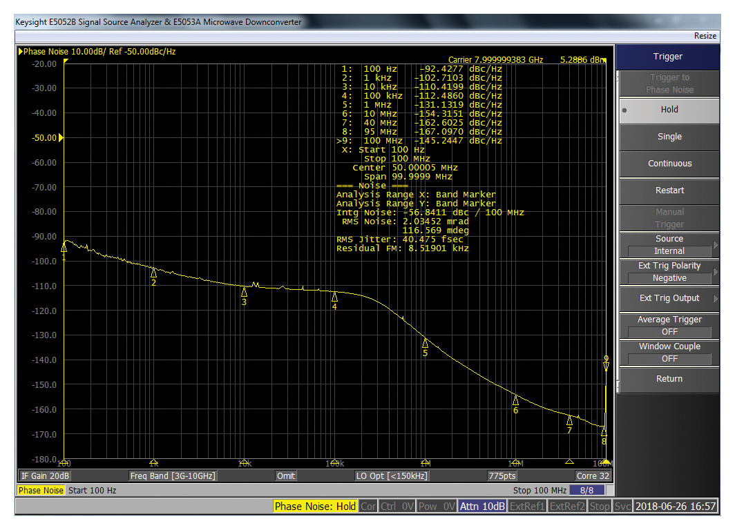
▲ RMS 지터: 8.0GHz [이미지=ADI]
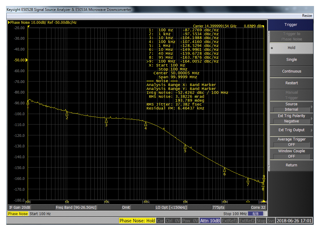
▲ RMS 지터: 14.4GHz [이미지=ADI]
통신 및 계측 애플리케이션용 LO
ADF5610은 무선통신 및 계측 애플리케이션용 LO로 사용하기에 적합한 특징들도 갖추고 있다. 분수 분해능(Fractional resolution)은 24비트로 보통이지만, ADF5610의 주파수 모드 기능과 결합하면 0Hz 오차의 주파수 생성이 가능하다.
LO로 ADF5610을 사용하면 출력 전력이 공칭 5dBm이기 때문에 능동 믹서를 RFOUT 포트로부터 직접 구동할 수 있다. 따라서 추가적인 증폭이 필요치 않아 보드 공간을 절약할 수 있다.
차동 분할기(PDIVOUT/NDIVOUT)의 출력 전력은 싱글 엔드로 사용하면 공칭 2dBm인데, 협대역 애플리케이션을 위해 저손실 발룬(balun)이나 하이브리드 커플러를 통해 결합하면 출력 전력을 몇 dB 더 높이거나 2배의 출력 전력을 달성할 수 있다.
700mW 미만(출력 분할기를 비활성화한 상태에서의 저전류 모드일 때)에서부터, 최악의 조건일 때에도 1W 조금 넘는 수준(출력 분할기를 128 분주로 설정한 상태에서의 고성능 모드일 때)밖에 소모하지 않는다는 점은 또 다른 장점이다.
저전류 모드에서도 위상 잡음 성능이 2dBc/Hz밖에 증가하지 않는다. 또한, PFD 스퓨리어스가 -105dBc로 낮고 대역내 필터링하지 않은 정수 경계 스퍼는 공칭 -45dBc이다.
추가적 디커플링 최소화한 소형 풋프린트 솔루션
ADF5610 PLL/VCO는 7mm × 7mm 48핀 LGA 패키지로 제공된다. 추가적인 디커플링은 최소한으로 필요하며, 소형 풋프린트 솔루션으로서는 최고의 성능을 제공한다.
최상의 성능을 달성해야 한다면 ADM7150, LT3045/LT3042, HMC1060 같은 고품질 LDO 레귤레이터를 사용할 것을 권장한다.
VCO는 5V 전원을 필요로 하고, 나머지 회로는 3.3V 레일로 구동된다. ADIsimPLL™로 ADF5610을 시뮬레이트 하면 전체 PLL 합성기를 구현하는데 필요한 적정 외부 회로를 설계할 수 있다.
결과적으로, ADI의 ADF5610은 설계 요건이 까다로운 최신 통신 및 계측 시스템에 사용하기에 적합하다.
이 기사는 아나로그디바이스의 마티 리처드슨(Marty Richardson) 선임 애플리케이션 엔지니어의 ‘멀티옥타브 주파수 커버리지와 탁월한 위상 잡음 성능 갖춘 마이크로파 합성기 IC(Microwave Synthesizer Offers Multioctave Frequency Coverage and Excellent Phase Noise Performance)’라는 제목의 글을 정리한 것입니다.