기사입력 2020.08.31 10:21
삼성전자가 제51기 정기 주주총회를 열고 지난해 경영 실적을 발표했다. 연결 기준으로 삼성전자의 2019년 경영 실적은 전년 대비 둔화한 매출 230조 원, 영업이익 28조 원이었다. 김기남 부회장은 AI 전용 반도체, 폴더블 폰 등 지속적인 기술 혁신과 더불어 미래 성장 기반 기술에 대한 투자를 통해 사업기회를 선점하겠다고 밝혔다.
2020-03-18 오전 10:31:23by 이수민 기자
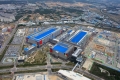
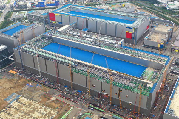
삼성전자가 EUV 기반 제품 수요에 대응하기 위해 경기도 평택캠퍼스에 파운드리 생산 시설을 구축한다고 밝혔다. 삼성전자는 이달부터 평택 파운드리 라인 공사에 착수했으며, 2021년 하반기부터 본격적으로 5나노 제품을 양산할 계획이다.
2020-05-21 오전 11:01:52by 이수민 기자
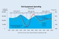
SEMI의 세계 팹 전망 보고서에 따르면, 2021년 반도체 팹 장비 투자액은 2020년 대비 약 24% 증가한 677억 달러에 이를 전망이다. 메모리 팹이 300억 달러 규모로 가장 큰 투자를 할 것으로 보이며, 로직 팹 및 파운드리가 290억 달러로 그 뒤를 이을 것으로 보인다.
2020-06-10 오후 1:01:50by 강정규 기자

[열린보도원칙] 당 매체는 독자와 취재원 등 뉴스이용자의 권리 보장을 위해 반론이나 정정보도, 추후보도를 요청할 수 있는 창구를 열어두고 있음을 알려드립니다.
고충처리인 장은성 070-4699-5321 , news@e4ds.com