Through pre-wet process and pulse partial plating
Supports high aspect ratio TSV processes without joints and seams ACM Research announced on the 3rd the 'Ultra ECP 3d Platform' for 3D Through-Silicon Via (TSV) technology.

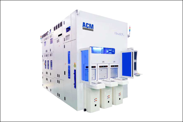
▲ Ultra ECP 3d platform [Photo = ACM]
The Ultra ECP 3d platform, leveraging ACM’s Ultra ECP ap and map platforms, provides copper (Cu) electroplating performance that leaves no defects such as voids or seams.
According to market research firm Mordor Intelligence, the 3D TSV equipment market size reached $2.8 billion in 2019 and is expected to grow at a compound annual growth rate of 6.2% to $4 billion in 2025.
Equipment utilizing TSV technology is used in the fields of memory, imaging, microelectromechanical systems (MEMS), and optoelectronics.
“The 3D TSV market is growing due to device miniaturization, AI, and edge computing technologies. These technologies require continuous improvement in chipset performance and integration, which is driving the adoption of TSV technology in more industries,” said David Wang, CEO of ACM.
Bottom-up (Bot) for High Aspect Ratio TSVDuring charging, the copper electrolyte must be able to completely fill the micropores without any bubbles inside, and a pre-wet step is used to accelerate this process.
“ACM has demonstrated with our customers that our Ultra ECP 3d platform can successfully fill high aspect ratio vias,” Wang said. “The stacked chamber design is engineered to deliver higher throughput while using fewer consumables, lowering total cost of ownership and improving fab space utilization.”
Measuring 2.2 m wide, 3.6 m long and 2.9 m high, the Ultra ECP 3d platform for 3D TSV is a 300 mm machine with 10 chambers that integrates pre-wet, copper plating and post-wet capabilities.
Recently, ACM delivered its first Ultra ECP 3D equipment to a Chinese customer and is currently validating 3D TSV and 2.5D interposer copper plating capabilities.