현재 파운드리 경쟁은 EUV 기술을 중심으로 전개 중이다. 파운드리 점유율 1위인 TSMC와 2위인 삼성전자만이 EUV 공정을 도입했기에 두 업체로 수요가 몰리는 상황이다. 삼성전자는 3nm에 3차원 구조인 GAA 기술 기반의 MBCFET을 도입할 예정이다. TSMC도 2nm 공정 이하부터는 삼성전자처럼 GAA 방식을 채택할 방침이다.
EUV로 미세화된 파운드리 공정, GAA로 3D화
삼성전자와 TSMC, '22년에 3차원 공정 경쟁
8인치 파운드리, 올해도 공급 부족 이어져
현재 파운드리 경쟁은 극자외선(Extreme Ultra Violet; EUV) 기술을 중심으로 전개 중이다. 파운드리 점유율 1위인 TSMC와 2위인 삼성전자만이 EUV 공정을 도입했기에 두 업체로 수요가 몰리는 상황이다.
한국반도체산업협회(KSIA)는 최신 리포트('21년 1월 11일)를 통해 3nm 공정 이후에는 3차원 구조 도입이 본격화될 것으로 예상했다.
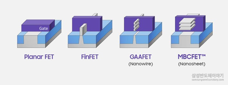
▲ 3차원 트랜지스터 구조의 발전 [출처=삼성전자]
삼성전자의 경우 3nm에 3차원 구조인 ‘GAA(Gate All Around)’ 기술 기반의 ‘MBCFET(Multi Bridge Channel FET)’을 도입할 예정이다. TSMC도 2nm 공정 이하부터는 삼성전자처럼 GAA 방식을 채택할 방침이다.
3차원 구조인 GAA 기술은 EUV 기술이 기반으로, 파운드리 기술 진입 장벽은 더욱 높아질 것이며, 이에 따라 파운드리 산업 내 TSMC-삼성전자 양강 체제는 더욱 공고해질 전망이다.
◇ GAA 기술, 나노시트 기술경쟁으로 발전 전망
삼성전자는 나노와이어(Nanowire) 방식 대신 나노시트(Nanosheet) 방식으로 트랜지스터 수직 적층 기술을 적용한 MBCFET 기술을 3nm 공정부터 도입하고 있다. 이미 3D NAND 분야서의 경험으로 수직적층기술 비법을 보유하고 있어 타사대비 기술 도입에 유리할 전망이다.
TSMC는 3nm까지는 기술 안정화를 위해 기존 EUV 기반의 FinFET 기술을 계속 사용할 것으로 보인다. 하지만 2nm 공정에 나노시트 방식의 3차원 트랜지스터를 삼성전자의 3nm 공정 도입 시점과 비슷한 시점에 추진하는 것을 검토하고 있는 것으로 알려졌다.
나노시트 기반 3차원 트랜지스터 도입은 양사 모두 2022년 전후에 이뤄질 전망이며, EUV 이후에도 치열한 기술경쟁이 펼쳐질 것으로 예상된다.
◇ 3차원 구조 형성을 위한 증착/에칭/CMP 공정 사용 늘 것
3차원 나노시트 방식의 MBCFET 공정은 순차적 적층이 필요하다. 3D NAND와 다른 점은 실리콘(Si)과 실리콘-저마늄(SiGe)을 에피택셜(Epitaxial) 방식으로 순차 적층한다. SiGe는 희생 막으로 적층 이후 에천트(Etchant)를 활용하여 제거하고, 필요한 게이트를 형성한다.
EUV 공정은 5nm까지는 사용량이 급증하나, 4nm 공정 이후로는 사용량이 둔화할 전망이다. 반면 3차원 구조 형성을 위해 증착, 에칭 및 CMP 공정 사용량이 확대될 것으로 예상된다.
◇ 8인치 파운드리, 수요 증가로 공급 부족 심화 여전
12인치 파운드리와 종합반도체기업(Integrated Device Manufacturer: IDM) 업체들은 주로 연산과 기억을 담당하는 로직과 메모리 제품들을 12인치에서 생산한다. 8인치 파운드리에서는 PMIC, DDI, CIS, 지문인식 센서 및 RF 칩과 같이 아날로그 칩과 센서 칩을 주로 생산한다.
최근 8인치 파운드리 공급 부족 심화 지속으로 대만 UMC, VIS 등은 8인치 파운드리 가격을 10% 이상 올리고 있다. 8인치 파운드리 공급 부족 이유로는 8인치 파운드리 수요는 지속 증가하는 반면, 어플라이드 머트리얼즈, 램리서치와 같은 반도체 장비업체들이 주로 12인치 장비를 중심으로 생산하기 때문이다.
8인치 장비 공급에 대한 장비업체들의 미온적인 반응은 파운드리들이 8인치 캐파를 늘리는 데 지장을 주고 있다. 추가로 미국의 중국 제재로 중국 파운드리 업체인 SMIC의 공급 제한도 지속돼 8인치 파운드리 공급 부족을 심화시킬 전망이다.