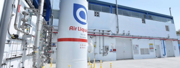
Air Liquide to Build 5,000N㎥/h Hydrogen Production Facility for Semiconductors in Taiwan
Korea produces 7,100N㎥/h of hydrogen for semiconductors, with additional expansion expected for EUV
Hydrogen for semiconductors is rapidly emerging as a key material in advanced EUV processes, and hydrogen production facilities for advanced semiconductor companies adopting EUV processes are being built one after another.
Air Liquide recently completed construction of the first phase of a 25MW water electrolysis hydrogen plant in Tainan and Hsinchu Science Park, Taiwan.
The ultra-pure hydrogen produced at this plant will be used exclusively for semiconductors, including by Taiwan's TSMC. The hydrogen production capacity is reportedly 5,000 N㎥/h.
The plant is known as a green hydrogen production facility that produces zero carbon dioxide emissions thanks to its water electrolysis facility that uses renewable energy. According to Air Liquide, it is expected to reduce carbon emissions by approximately 35,000 tons per year compared to typical hydrogen production facilities.
Air Liquide said it will continue construction of its hydrogen electrolyzer plant in Taiwan, from Phases 2 to 5, with a total capacity of 25 MW over the next two years.
The reason this plant is attracting particular attention is because it is expected to be used 100% for semiconductor hydrogen, and TSMC is expected to use almost all of the hydrogen produced at this plant.
According to local Taiwanese officials, in addition to the hydrogen it receives from this plant, TSMC is also planning to purchase land in the Nanguosugou Park and build two hydrogen production facilities using natural gas as a raw material.
TSMC is expected to use hydrogen for semiconductors mostly in its EUV equipment.
According to the industry, in the case of EUV equipment, a large amount of hydrogen is known to be used as atmospheric gas around the tin liquid when a CO₂ or YAG (yttrium, aluminum, garnet) laser is irradiated on the tin (Sn) liquid to generate ultra-fine EUV light.
For EUV equipment, the LPP (Laser Produced Plasma) method is used. When using an EUV exposure device, tin is melted and tin droplets are formed, which are then irradiated with a CO₂ laser or YAG laser. During this process, a large amount of reducing gas is required as atmospheric gas to prevent tin from being oxidized, and the most suitable reducing gas is hydrogen.
In this case, the large amount of tin and hydrogen used is said to produce stannane (SnH₄), which is insoluble in water and flammable, and a new exhaust method is required to deal with it.
It is also known that hydrogen can be used to clean EUV exposure equipment.
As of now, semiconductor manufacturers that have fully introduced and used EUV include Samsung Electronics in Korea and TSMC in Taiwan.
While most semiconductor manufacturers are sourcing hydrogen for semiconductors from external sources, Samsung Electronics in Korea exclusively receives hydrogen for semiconductors through pipelines from Linde Korea and Air Products Korea’s Giheung and Pyeongtaek production facilities.
The domestic production volume of hydrogen for semiconductors is estimated to be approximately 7,100 N㎥/h, and the actual distribution volume is estimated to be higher.
Considering that the recently built semiconductor hydrogen production facility in Taiwan has a capacity of 5,000 N㎥/h, it is analyzed that the domestic semiconductor hydrogen usage is greater.
In particular, since Korea currently does not have its own hydrogen production facilities for SK Hynix, if the spread of EUV increases further, Samsung Electronics and SK Hynix are expected to expand their own hydrogen production facilities, and hydrogen production for semiconductors is expected to increase further and remain the largest in the world.
Meanwhile, TSMC, Taiwan's largest carbon emitter, has shown keen interest in this water electrolysis hydrogen production facility, stating that hydrogen is key to its future transformation into an advanced semiconductor production company.