기사입력 2021.06.09 12:00
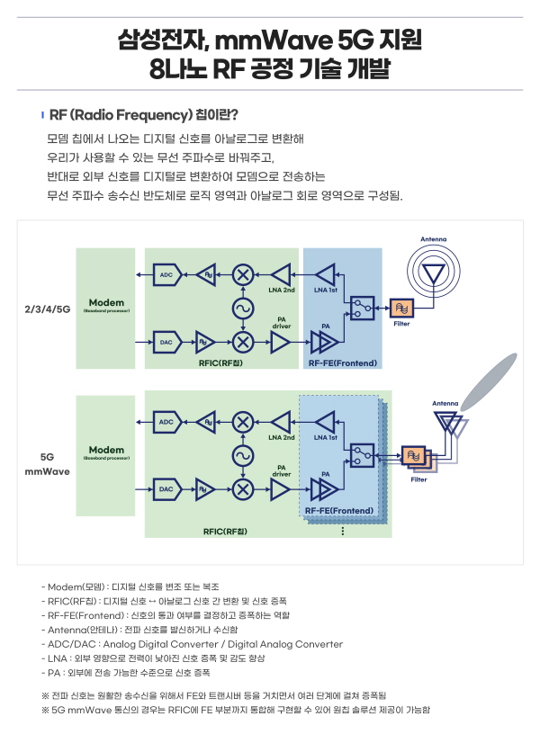
삼성전자가 차세대 인터페이스, 컴퓨트 익스프레스 링크(CXL) 기반 D램 메모리 기술을 개발했다고 밝혔다. CXL은 고성능 컴퓨팅 시스템에서 CPU와 함께 사용되는 가속기, 메모리, 저장장치 등을 보다 효율적으로 활용하기 위해 제안된 인터페이스로, 기존 컴퓨팅 시스템의 메모리 용량의 물리적 한계를 극복하고 D램의 용량을 확장할 수 있다.
2021-05-12 오전 8:22:20by 이수민 기자
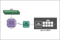
삼성전자가 시스템반도체 리더십 조기 확보를 위해 ‘시스템반도체 비전 2030’ 발표 당시 수립한 133조원의 투자계획에 38조원을 추가해 2030년까지 총 171조원을 투자하고 첨단 파운드리 공정 연구개발과 생산라인 건설에 더욱 박차를 가한다.
2021-05-14 오전 8:57:54by 배종인 기자
삼성전자가 DDR5 D램 모듈의 성능을 높이고 전력 사용을 줄이는 PMIC 3종을 공개하며, 시스템반도체 라인업을 확대한다. PMIC를 외부 기판에 탑재하던 DDR4 D램과 달리, DDR5 D램부터는 PMIC를 D램 모듈 기판에 직접 탑재한다. PMIC와 D램이 하나의 모듈에 있어 전원을 안정적이고 빠르게 공급해 메모리 성능 향상과 동시에 오작동을 최소화할 수 있다.
2021-05-18 오전 11:00:19by 이수민 기자

[열린보도원칙] 당 매체는 독자와 취재원 등 뉴스이용자의 권리 보장을 위해 반론이나 정정보도, 추후보도를 요청할 수 있는 창구를 열어두고 있음을 알려드립니다.
고충처리인 장은성 070-4699-5321 , news@e4ds.com


