전원공급장치, 저전압 고출력 구현 필요성 커져
ADI 3A 'LT3033' VLDO 레귤레이터 병렬연결로
출력 전류 3A 이상으로 높이고, 열 분산도 가능해
오늘날 컴퓨팅 시스템은 과거보다 많은 총 전력과 낮은 공급 전압을 요구한다. 따라서 전원공급장치 설계자는 좁은 공간에서 높은 출력 전류를 구현해야 한다.
낮은 출력 전압과 높은 전력 밀도에서 열 발산 문제는 설계 최우선 고려 사항이다. 특히 저잡음 애플리케이션의 선형 레귤레이터일 경우는 더욱 그렇다. 만약 LDO 레귤레이터를 병렬로 연결하면, 공급 전류 용량을 늘리고 열 발산을 완화해 특정 부품의 온도 상승을 낮추고, 필요한 냉각 장치 크기와 수를 줄일 수 있다.
ADI의 3A ‘LT3033’ 초저전압 강하 레귤레이터(VLDO)를 병렬 연결하면, 3A보다 높은 전류가 필요한 애플리케이션을 구동할 수 있다. 동시에 열도 분산한다. 또한, LT3033은 출력 전류 모니터링 기능을 내장해 전류 균형을 맞추기도 쉽다.
LT3033은 1.14V에서 10V까지의 입력 전원을 최대 3A 부하 전류 및 최저 0.2V 출력으로 변환한다. 강하 전압은 전체 부하에서 단 95mV다. 대기 전류는 동작 중에는 1.8mA고, 셧다운 시 22µA로 떨어진다. 프로그래밍 가능한 전류 제한과 열 보호 기능은 고전류 저전압 애플리케이션에 필요한 견고성을 제공한다.
◇ 3A, 단일 VLDO 애플리케이션 예시
1.2V 입력에 3A, 0.9V를 공급하는 LT3033은 안전성을 위해 IN/OUT 핀에 최소 10µF의 ESR 세라믹 커패시터가 필요하다. VOUT과 ADJ 핀 사이에 순방향 커패시터(CFF)를 추가하면, 과도 응답은 높이고 출력 전압 잡음은 낮출 수 있다.
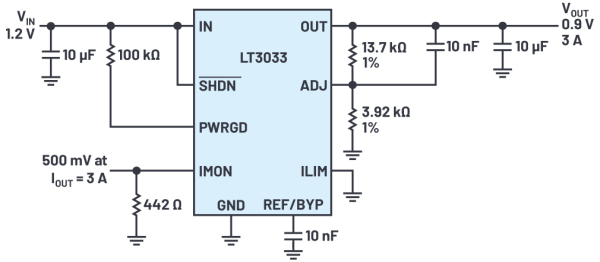
▲ 일반적인 LT3033 애플리케이션 [그림=ADI]
REF/BYP 핀과 GND 사이에 10nF 바이패스 커패시터를 사용하면 일반적으로 10Hz~100kHz 대역폭에서 출력 전압 잡음을 60µVrms로 낮추고, 기준전압을 소프트 스타트 할 수 있다. 레귤레이션에 필요한 최소 입력 전압은 조절된 출력 전압 VOUT에 강하 전압을 더한 값이나 1.14V 중 큰 값과 같다.
전류 제한은 단일 저항을 ILIM 핀에서 GND로 연결하여 프로그래밍할 수 있으며, 넓은 온도 범위에서 ±12%의 정확도를 갖는다. 외부 전류 제한은 입출력의 차동 전압이 5V를 넘으면 폴드백 내부 전류 제한 때문에 오버라이드 될 수 있다.
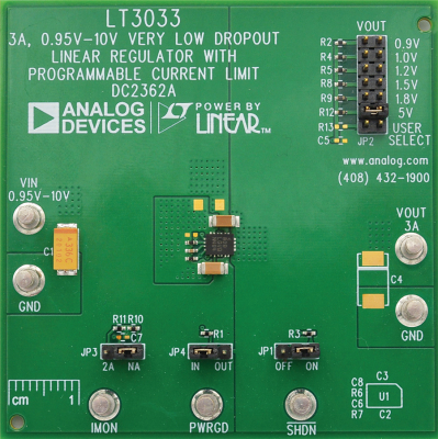
▲ LT3033 데모 보드 [사진=ADI]
LT3033은 저항을 통해 IMON 핀을 GND로 구동하여 출력 전류 모니터를 제공한다. IMON 핀은 PNP의 콜렉터로서, LT3033 출력 PNP를 1:2650의 비율로 미러링한다. 저항 전압은 VOUT-400mV보다 높지 않으면 출력 전류에 비례한다.
IOUT = 2650 × (VIMON / RIMON)
이 출력 전류 모니터는 여러 개의 LT3033 디바이스가 전류를 공유할 수 있게 한다. 크기는 작지만, LT3033은 폴드백 내부 전류 제한, 열 제한, 역전류 및 역극성 배터리 보호를 포함한 여러 보호 기능들을 포함하고 있어 유용하다.
◇ 6A 애플리케이션을 위한 LT3033 2개 병렬연결
3A 이상이 필요한 애플리케이션은 여러 LT3033을 병렬연결해 지원할 수 있다.
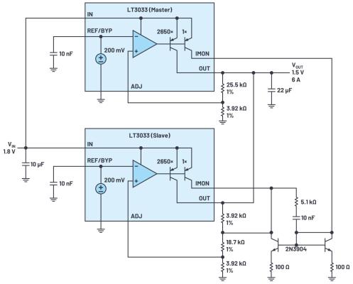
▲ 2개의 2N3904 NPN 디바이스와 함께
병렬연결한 2개의 LT3033 [그림=ADI]
위의 그림은 2개의 2N3904 NPN 디바이스와 2개의 LT3033을 병렬 연결해 1.5V, 6A 출력을 생성하는 방법을 나타낸 것이다. 개별 IN 핀과 OUT 핀은 각각 함께 연결된다. 1개의 마스터 LT3033은 슬레이브 LT3033을 제어한다.
IMON 핀은 NPN 전류 미러와 결합해 증폭기를 생성한다. 이 증폭기는 슬레이브 LT3033의 피드백 분배기로 전류를 주입, 각 LT3033의 IMON 전류를 같게 한다.
100Ω 저항은 전체 부하에서 113mV 이미터 디제너레이션을 제공하므로 우수한 전류 미러 정합을 보장한다. 슬레이브 LT3033의 출력 전압은 마스터 LT3033이 제어 상태를 유지하도록 회로 출력보다 10% 낮은 1.35V로 설정된다.
슬레이브 LT3033의 피드백 저항은 섹션으로 분리되어 슬레이브 NPN의 적절한 헤드룸을 보장한다. 슬레이브 디바이스의 IMON 핀에 추가된 10nF, 5.1kΩ 커페시터와 저항의 조합은 피드백 루프를 주파수 보상한다.
이 회로는 6A 부하 전류를 공급할 수 있지만, 전류 공유 정확도는 2개 NPN 디바이스 간의 부정합에 의해 제한된다. 이런 부정합은 보드에 균일하지 않은 열 분포를 발생시킨다. ADI의 ‘MAT14’와 같은 정합 모놀리식 트랜지스터를 사용하여 2개의 디스크리트 NPN 디바이스를 대체하면 더 정확한 전류 공유가 가능하다.
.jpg)
▲ MAT14 정합 모놀리식 쿼드 트랜지스터와
병렬 LDO 레귤레이터를 사용하면
정류 공유 부정합을 줄일 수 있다 [그림=ADI]
MAT14는 높은 파라메트릭 정합을 제공하는 쿼드 모놀리식 NPN 트랜지스터로, 최대 전류 이득 정합은 4%이다. 2N3904와 비교할 때, MAT14 전류 미러는 전류 부정합을 5.3%에서 1.6%로 낮춘다. 위는 디스크리트와 정합 NPN 디바이스를 사용하는 LDO 레귤레이터의 출력 전류를 비교한 것이다.
◇ 정합 부품을 이용한 LT3033 4개 병렬연결
이 병렬연결 회로 아키텍처는 전류 미러를 확장하고, 슬레이브 LT3033 디바이스를 추가함으로써, LT3033을 필요한 만큼 많이 확장할 수 있다.
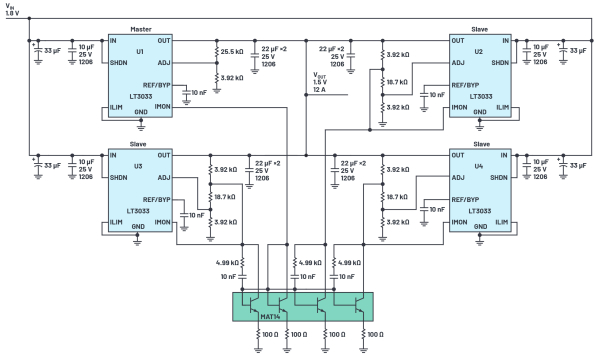
▲ MAT14로 병렬 연결한 4개 LT3033 [그림=ADI]
위는 전류 공유를 위해 MAT14를 사용하여 LT3033 4개를 병렬연결한 예시다.
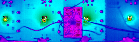
▲ 병렬 연결한 4개 LT3033의 열 성능 [사진=ADI]
위는 열 성능이다. LT3033 4개는 온도가 51~58°C 수준이다. 각 부품에 대한 입력 트레이스를 따라 발생하는 전압 강하를 고려할 때, 열이 보드에 균일하게 확산하므로, 솔루션에 균등한 전류 공유가 이루어진 것으로 볼 수 있다.
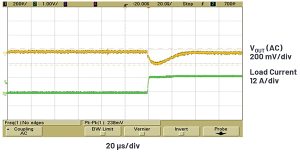
▲ 병렬 연결한 4개 LT3033의 부하 과도 응답 [=ADI]
위는 1.8V 입력으로 동작하는 1.5V 출력, 12A 전원 공급장치의 과도 응답이다.
◇ LT3033, 스위칭 레귤레이터와 전기 효율 비슷
LT3033은 3 × 4mm 패키지로 제공되는 3A VLDO 레귤레이터로, 출력 전류 모니터링 기능이 내장되어 고전류 애플리케이션을 위해 병렬연결이 가능하다. 전체 부하에서 전압 강하가 95mV에 불과하여 낮은 입출력 전압, 높은 전류 애플리케이션에 적합하며, 스위칭 레귤레이터에 견줄 만한 전기 효율을 달성한다.
그 외에도 신뢰할 수 있는 견고한 솔루션을 위한 프로그래밍 가능한 전류 제한, 전원 양호 표시, 열 제한 기능 등을 포함하고 있다. 배터리로 구동하는 시스템을 개발하는 엔지니어는 낮은 대기 전류와 역극성 배터리 보호를 실현할 수 있다.
해당 기사는 아나로그디바이스(ADI)의 몰리 주(Molly Zhu) 선임 애플리케이션 엔지니어, 페이 구오(Fei Guo) 필드 애플리케이션 엔지니어가 함께 저술한 '출력 전류를 늘리고 열 발산을 완화하기 위한 VLDO 레귤레이터 병렬연결 방법(Paralleling Very Low Dropout Linear Regulators for Increased Output Current and Even Heat Distribution)'이라는 제목의 글을 정리한 것입니다.