기사입력 2021.06.25 09:51
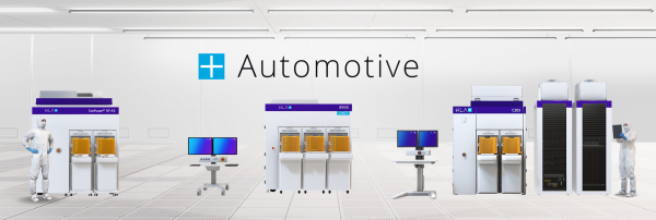
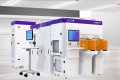
KLA가 최첨단 메모리 및 로직 집적 회로 제조 문제 해결을 위해 설계한 'PWG5 웨이퍼 기하 구조 계측 시스템'과 '서프스캔 SP7XP 웨이퍼 결함 검사 시스템'을 발표했다. PWG5는 고해상도로 웨이퍼 기하 구조의 미세한 변형을 측정해 패턴 웨이퍼 변형을 식별하고 수정한다. 서프스캔 SP7XP는 머신 러닝 기반 결함 분류 기능을 도입해 넓은 범위의 박막, 기판 등에서 다양한 결함을 검출하고 식별할 수 있다.
2020-12-15 오전 10:39:38by 이수민 기자

삼성전자의 NXP 반도체 인수 가능성을 점쳐보는 기사들이 쏟아지고 있다. 과거 NXP가 자사의 매각을 시도한 적이 있었고, 삼성전자가 3년 내로 의미 있는 인수·합병을 추진하겠다고 선언했기 때문이다. 하지만 차량용 반도체 사업의 수익성이 생각보다 크지 않기 때문에 가능성은 크지 않다.
2021-04-29 오후 2:45:57by 이수민 기자
전 세계적인 차량용 반도체 공급 불안정에 국내 자동차부품업체 다수가 경영상 어려움을 겪고 있는 것으로 드러났다. KAIA가 지난 3~4일 국내 완성차업체 1~3차 협력사인 부품업체 78곳을 대상으로 실시한 긴급 실태조사에 따르면, 조사업체의 84.6%(66개 사)가 반도체 수급과 이로 인한 완성차업체의 생산자질로 인해 경영 애로를 겪고 있다고 답했다.
2021-05-11 오전 9:30:30by 이수민 기자

[열린보도원칙] 당 매체는 독자와 취재원 등 뉴스이용자의 권리 보장을 위해 반론이나 정정보도, 추후보도를 요청할 수 있는 창구를 열어두고 있음을 알려드립니다.
고충처리인 장은성 070-4699-5321 , news@e4ds.com


