IBS 다차원 탄소 재료 연구단이 2차원 흑린으로 0.43nm 선폭의 전도성 채널을 구현했다. 2차원 흑린은 포스트 그래핀 시대의 주력 반도체 소자로 꼽힌다. 두께가 원자 한 층 정도로, 실리콘 기반 반도체로 구현하기 힘든 유연하고 투명한 소자에 이용할 수 있다. 또한 2차원 반도체 소자 중 전자이동도가 가장 크다.
선폭 가늘수록 반도체 고성능 "5nm 이미 상용"
IBS 연구단, 선폭 0.43nm 전도성 채널 구현
2nm 이하에서 기본 소자 구조 형성 가능 입증
반도체는 회로 선폭을 가늘게 만들수록 단위 면적당 더 많은 소자를 집적할 수 있어 성능 향상이 가능하다. 최근 업계는 선폭이 5nm(나노미터) 정도인 반도체의 상용화에 들어섰으며, TSMC, 삼성전자, 인텔 등은 더욱 미세화에 고심 중이다.
기초과학연구원(IBS) 다차원 탄소 재료 연구단 이종훈 그룹리더(UNIST 교수)와 펑딩 그룹리더(UNIST 교수) 연구팀은 30일, 2차원 흑린으로 선폭 4.3Å(0.43nm)의 전도성 채널을 구현했다. 나노미터 한계를 뛰어넘어 옹스트롬(Å, 0.1nm) 단위 선폭의 초 극미세 반도체 소자 가능성을 실험적으로 제시한 것이다.
▲ 1나노미터 단위 수준의 반도체 소자 [사진=IBS]
이번 연구는 울산과학기술원(UNIST), 포항공대(POSECH)와 공동으로 진행했다.
2차원 흑린은 포스트 그래핀 시대의 주력 반도체 소자로 꼽힌다. 두께가 원자 한 층 정도로, 실리콘 기반 반도체로 구현하기 힘든 유연하고 투명한 소자에 이용할 수 있다. 또한 2차원 반도체 소자 중 전자이동도가 가장 크다. 그래핀과 달리 밴드 갭(band gap)이 있어 전기를 통하게 했다가 통하지 않게 하는 제어도 쉽다.
그간 흑린 등 2차원 물질들을 반도체 소자로 활용하려는 시도들이 많았다. 하지만 실제 소자화하는 공정 과정에서 발생하는 결함(defect)에 관한 연구는 미비했다.
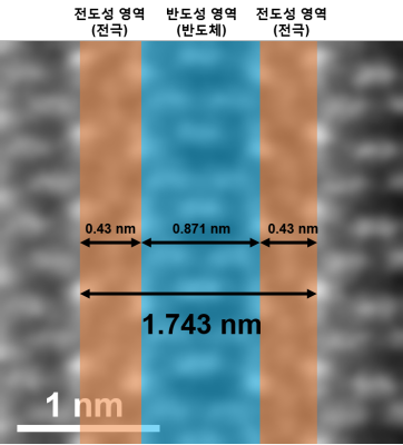
연구진은 전극으로 활용될 수 있는 전도성 채널을 만들고자 다층의 2차원 흑린 각 층 사이에 구리 원자를 삽입했다. 이때 흑린에 얇은 구리 박막을 증착한 후 열처리를 하는 간단한 공정을 진행한다. 그러면 흑린의 이방성 원자구조로 인하여 구리 원자가 2차원 흑린에 0.43nm의 미세한 폭을 유지하며 삽입된다.
0.43nm 두께의 전도성 채널은 반도체 소자의 전극으로 사용될 수 있다. 연구진은 또한 전도체-반도체-전도체로 이뤄진 반도체 기본 소자 구조를 2nm 이하 수준에서 형성할 수 있음도 원자 분해능 투과전자현미경(TEM)으로 증명했다.
제1 저자인 이석우 연구원은 이번 성과에 대해 “흑린을 이용한 초미세 반도체 소자 실현 가능성을 보여줬다”라며, “현재 반도체 공정에 사용될 수 있는 고상 확산법을 이용하였기 때문에 실제 응용 효과가 클 것”이라고 설명했다.
이종훈 그룹리더는 “흑린은 2차원 반도체 소자 분야에서 그래핀을 능가할 물질”이라며, “초 극미세 소자로서의 활용 가능성을 확인했다”라고 말했다. 연구 결과는 7월 29일, 나노레터스(Nano Letters, IF 11.189) 표지논문으로 게재됐다.
.jpg)