
기사입력 2022.02.07 12:26
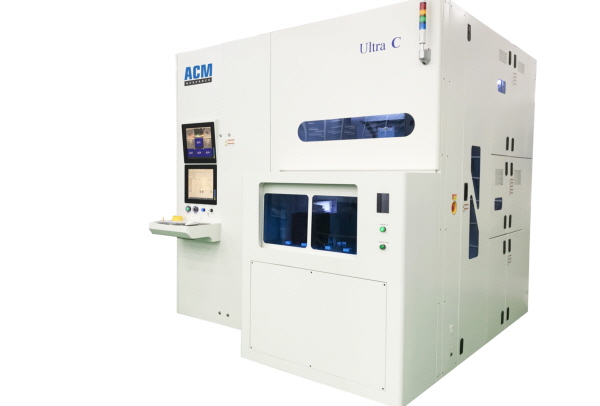
반도체 및 고급 WLP(Wafer-Level Packaging) 애플리케이션용 웨이퍼 처리 솔루션의 선도 기업인 ACM 리서치(ACM Research, Inc.)가 글로벌 주요 반도체 제조사로부터 SAPS 데모 장비 수주를 통해 비즈니스 및 협력의 기회를 넓혀나가고 있다.
2021-11-10 오후 4:49:50by 배종인 기자
반도체 및 고급 WLP(Wafer-Level Packaging) 애플리케이션용 웨이퍼 처리 솔루션의 선도 기업인 ACM 리서치(ACM Research, Inc.)가 주요 IC 제조사로부터 ECP 데모 장비를 수주하며 고객 확대에 적극 나서고 있다.
2021-11-16 오후 4:50:16by 배종인 기자

반도체 및 고급 WLP(Wafer-Level Packaging) 애플리케이션용 웨이퍼 처리 솔루션의 선도 기업인 ACM 리서치(ACM Research, Inc.)가 중국 소재 글로벌 종합반도체 기업(IDM)으로부터 첫 수주를 이끌어냈다.
2021-11-23 오후 4:11:47by 강정규 기자


[열린보도원칙] 당 매체는 독자와 취재원 등 뉴스이용자의 권리 보장을 위해 반론이나 정정보도, 추후보도를 요청할 수 있는 창구를 열어두고 있음을 알려드립니다.
고충처리인 장은성 070-4699-5321 , news@e4ds.com
