김형섭 삼성전자 연구소장, “반도체 혁신 무한 협력 必”
기사입력 2022.02.09 14:21
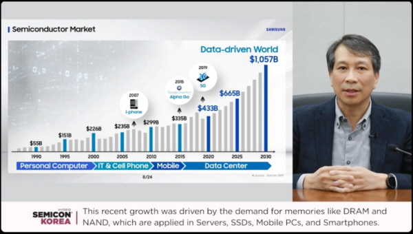
9일 개막 ‘세미콘 코리아 2022’ 기조연설
초연결시대, 반도체 혁신 위한 협력 필수
김형섭 삼성전자 반도체연구소 연구소장이 반도체 혁신을 위해 업계뿐만 아니라 학계와 정부기관 등 무한한 협력을 요청했다.
김 소장은 9일 개막한 '세미콘 코리아 2022' 온라인 기조연설에 나서 한계기술 극복을 위한 협력을 역설했다.
그는 “구조, 공정, 설비, 소재 분야의 기술 혁신과 한계 기술에 대한 도전이 없었다면 반도체 산업은 성장할 수 없었을 것”이라며 “미래에는 더 많은 혁신이 필요할 것이고, 이는 학계, 정부기관, 소재사 등의 무한한 협력을 통해 가능하리라 믿는다”고 전했다.
코로나19 팬데믹으로 대면활동이 제한됨에 따라 의료 서비스, 화상 업무 및 수업 등 물리적으로 접촉하며 행하던 활동이 비대면으로 대체되었다.
이는 비대면 연결에 필요한 인프라의 확충, 관련 서비스의 성장과 문화 변화로 이어졌고 초연결시대로 이어졌다.
현재 주변의 수많은 기기들은 5G, 블루투스, 와이파이와 기타 데이터 통신이 가능한 모듈을 통해 실시간으로 연결되고 이러한 기술은 급속도로 증가하는 추세다.
기기간 연결의 증가는 데이터의 폭증으로 이어진다.
현재 1년에 약 64ZB의 데이터가 생성되는 반면 2025년에는 3배에 달하는 181ZB 데이터가 생성될 것으로 전망된다.
데이터 폭증에 따른 반도체의 수요도 증가했고, 업계는 지속적 성장을 기대하고 있다.
반도체 시장의 매출은 지속적으로 증가하고 있으며, DRAM, NAND와 같은 메모리 분야에 의해 주도되어 왔다.
초연결시대는 반도체 없이는 불가능했고, 현재와 미래에도 반도체는 필수 요소라는 것이 김 소장의 설명이다.
수요 증가와 함께 성능 개선의 요구를 충족시키기 위한 반도체 기술 혁신도 뒤따랐다.
로직, DRAM, 플래시 분야에서는 트랜지스터를 작게 만들어 소재의 밀도를 높이고, 저전력 환경에서 구동될 수 있도록 개발해왔다.
트랜지스터는 초고층 형태로의 구조적 변화와 전기 용량 극대화를 위한 유전체 물질도 연구됐다.
CIS의 고집적화에 따른 픽셀 당 포톤의 감소와 픽셀 간 간섭에 의한 노이즈 증가는 소자 구조 개선을 통해 극복했다.
이에 멈추지 않고 반도체의 혁신을 위해 제품의 구조 자체를 변경하려는 시도를 하고 있다고 김 소장은 밝혔다.
DRAM은 셀 트랜지스터의 구조를 변경하거나 컴패시터를 없애는 기술을 연구하고 있고, 로직 분야에서는 소모 전력 감소와 성능 향상을 위해 파워 네트워크를 웨이퍼 뒷면에 배치하는 기술을 학계와 제조 업계에서 연구하고 있다.
그 중 Atomic Layer Etch는 식각 대상물을 원자 단위로 식각하는 기술로, 미세 패턴 패터닝 시 요구되는 세밀한 식각 정밀도와 균일도를 만족시킬 수 있는 기술이다.
한편 김 소장은 친환경에 대한 의무감도 나타냈다.
그는 “전 세계 CO2 배출량의 약 60%가 산업체와 에너지 생산과정에서 발생되고 있다”며 “제품을 생산할 때 많은 에너지 사용 및 부산물 배출은 업계가 고민하고 노력해야 한다”고 전했다.

관련뉴스
-
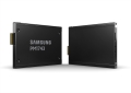
삼성전자, PCIe 5.0 고성능 SSD로 속도 2배 ↑
삼성전자가 업계 최고 수준의 PCIe 5.0 기반의 고성능 SSD를 출시하며 PCIe 4.0 대비 읽기·쓰기 속도를 약 2배로 개선하며, 고성능 SSD 시장 개척에 나섰다.
2021-12-26 오후 4:25:24by 배종인 기자
-

삼성전자, 세계 최초 MRAM 저전력 설계 성공
삼성전자가 기존 MRAM의 한계를 뛰어넘어 저전력 설계에 성공해 차세대 저전력 AI 칩 기술의 지평을 확장했다. 삼성전자 연구진이 MRAM을 기반으로 한 인-메모리(In-Memory) 컴퓨팅을 세계 최초로 구현했다.
2022-01-13 오전 8:41:05by 성유창 기자
-
.jpg)
삼성전자, 게임성능·머신러닝 둘 다 잡은 모바일AP
삼성전자는 약점이었던 경쟁사 대비 높은 전력소모와 GPU 성능을 보완한 모바일AP ‘엑시노스2200’을 공개했다.
2022-01-19 오전 8:30:30by 성유창 기자

많이 본 뉴스

[열린보도원칙] 당 매체는 독자와 취재원 등 뉴스이용자의 권리 보장을 위해 반론이나 정정보도, 추후보도를 요청할 수 있는 창구를 열어두고 있음을 알려드립니다.
고충처리인 장은성 070-4699-5321 , news@e4ds.com