Unique iToF BSI technology based on 40㎚
Supporting high performance with low power and small sensors
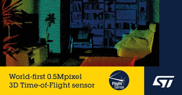
STMicroelectronics, a global semiconductor leader serving customers across the spectrum of electronics applications, has introduced the industry’s first 0.5-megapixel depth image sensor that revolutionizes digital vision.
STMicroelectronics today announced a new family of high-resolution time-of-flight (ToF) sensors that bring advanced 3D depth imaging to smartphones and other devices.
This 3D product family includes the VD55H1, which measures distances using over 500,000 points to map three-dimensional surfaces.
The sensor detects objects up to 5 meters away, and can be used with patterned lighting to detect objects at even greater distances.
The VD55H1 enables new AR/VR market applications such as room mapping, gaming, and 3D avatars. Applying this sensor to smartphones will improve the performance of camera system functions such as bokeh effect, multi-camera selection, and video splitting.
Additionally, by improving facial authentication security with higher resolution and more accurate 3D images, it can protect all smart systems related to secure transactions and access control, including phone unlocking, mobile payments.
For robotics, the VD55H1 provides high-fidelity 3D scene mapping over any target distance, enabling new and more powerful capabilities.
“The innovative VD55H1 3D depth sensor reinforces ST’s leadership in ToF and complements our overall offering of depth-sensing technologies,” said Eric Aussedat, Executive Vice President, General Manager, Imaging Subgroup, STMicroelectronics. “The FlightSense™ portfolio now extends from single-point ranging sensors to sophisticated, high-resolution 3D imagers that enable the next generation of intuitive, autonomous, and smart devices with our indirect Time-of-Flight (iToF) and direct Time-of-Flight (dToF) products.”
iToF sensors, such as the VD55H1, calculate the distance to an object by measuring the phase shift between the reflected and emitted signal. This is a complementary technology to dToF sensors, which measure the time it takes for a transmitted signal to reflect back to the sensor. ST designs high-resolution dToF and iToF sensors with a broad portfolio of advanced technologies, providing optimized solutions to meet application requirements.
Leveraging its own 40nm stacked wafer technology, the VD55H1 features a unique pixel architecture and manufacturing process to ensure low power consumption, low noise, and optimized die area. The die contains 75 percent more pixels than conventional VGA sensors in a smaller die size.
The VD55H1 sensor is currently sampling to lead customers, with volume production scheduled for the second half of 2022. Reference designs and full software packages are also available to accelerate sensor evaluation and project development.