[연재]ST 유지 카와노 엔지니어(17)-“노이즈 차단·규정 전압, 래치업 방지 핵심”
기사입력 2022.04.05 10:51
“노이즈 차단·규정 전압, 래치업 방지 핵심”
외부노이즈·전압변경 게이트노이즈, 래치업 원인
MCU 수많은 PNPN 접합, 원인접합 예상 불가능
외부노이즈·전압변경 게이트노이즈, 래치업 원인
MCU 수많은 PNPN 접합, 원인접합 예상 불가능
[편집자주]일반적으로 반도체라 하면 컴퓨터의 CPU와 메모리처럼 일반인에게 익숙한 반도체를 떠올리기 마련이다. 반면에 전자제품 구동을 위해서 핵심 반도체로 쓰이는 MCU(Micro Controller Unit)의 경우 일반적으로 우리가 쉽게 접하는 모든 전자제품에서 사용되고 있으면서도 일반인에게는 아직 낯선 반도체다. 이런 MCU가 최근 반도체 부족 사태로 인해 언론에 오르내리며, 일반인들에게 주목받기 시작했다. 이에 본지는 MCU 반도체 전문기업인 ST마이크로일렉트로닉스의 유지 카와노 매니저의 연재기고를 통해 MCU에 대해 전문적으로 알아보는 자리를 마련했다.
 ■ 질문
■ 질문MCU에서 어떤 종류의 래치업이 발생하는 경향이 있는가?
■ 답변
MCU는 많은 수의 PN 접합으로 구성되어 있으며, 일부는 4중-레이어 PN 접합(PNPN 접합)을 형성하고 있고, 이것은 다시 기생 사이리스터(parasitic thyristor)를 구성한다.
사이리스터는 전력 제어를 위한 스위칭 소자이다. 이것은 양극(anode), 음극(cathode), 게이트의 3단자로 구성되어 있다.
일반적인 상태에서 양극에서 음극으로 전혀 전류가 흐르지 않지만, 게이트에 신호가 인가되면, 전류가 양극에서 음극으로 흐르게 된다.
일단 전류가 흐르기 시작하면, 전력이 차단되기 전까지 중단되지 않는다.
대전류(large current)를 통과시키기 위해서는 온-저항이 매우 작아야 한다. 동일한 현상이 MCU 내부의 기생 사이리스터에서 발생할 수 있으며, 이러한 현상을 래치업이라고 한다.
MCU 내부의 래치업 이벤트는 대전류를 생성하며, 이것은 고장을 일으킬 뿐만 아니라 최악의 경우에 배선을 녹이거나 내부 MCU의 구성요소들을 파괴할 수 있다.
래치업은 정상 사용 시에는 발생하지 않지만 전원 동작 시의 에러 또는 터미널 상에서 고전압 노이즈의 급격한 상승 등으로 인해 이러한 현상이 유도될 수 있다. 그림 1은 MCU 표면의 금속선이 래치업으로 인해 녹아버린 사진이다.
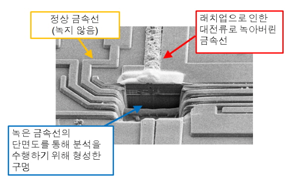
▲그림1 : 금속선을 녹이는 원인이 되는 래치업
■ 설명
○ 사이리스터 구조
그림 2(a)는 PNPN 사이리스터의 구조를 나타낸 것이다. 양의 전압이 양극에 인가되고 음의 전압이 음극에 인가되면, 양극에서 음극으로 전류가 전혀 흐르지 않는다. 이것은 역전압(backward voltage)이 J2에 인가되고, 순전압(forward voltage)이 J1과 J3에 각각 인가되기 때문이다.
하지만 전압을 게이트에 인가하여 전류를 통과시킬 수 있다면, 그 결과 게이트 전류가 J2를 통과하는 역전류를 상승시키고 전류의 양을 상당히 증가시켜 양극에서 음극으로 이것이 흐르게 된다. 이것은 순전압이 J1과 J3 각각에 이미 인가되고 있기 때문이다. 일단 전류가 흐르기 시작하면 양극에 대한 전력 공급이 중단될 때까지 지속된다.
이것은 사이리스터의 스위칭 동작을 설명한 것으로 전력 장비의 스위칭 소자로 사용된다.
그림 2(b)에 나타낸 바와 같이 PNPN 접합은 PNP 트랜지스터와 NPN 트랜지스터를 통합한 것과 같다. 이 2-트랜지스터 구조를 그림 2(c)의 회로 다이어그램에 나타냈다.
Tr1 이미터 (E)가 사이리스터의 양극으로서 동작한다. 베이스는 Tr1 콜렉터 (C) (Tr2 베이스 (B))이다. Tr2 이미터 (E)가 사이리스터의 음극으로서 동작한다.
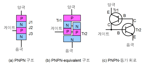
▲그림 2 : 사이리스터 구조
MCU의 CMOS 구조에서 이들 2개의 트랜지스터를 그림 3에 나타냈다.
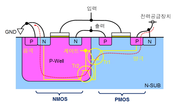
▲그림 3 : 래치업 이벤트 메커니즘
○ 래치업 이벤트 메커니즘
N-SUB(그림 3 참조)와 P-SUB 모두 결과적으로 기생 PNPN 접합 구조를 형성하며, 래치업 이벤트 메커니즘은 양쪽 모두 동일하다.
Tr1은 전원공급장치에 연결된 PMOS 소스 Pch, N-SUB, 그리고 P-WELL로 이루어진 회로로 구성된다. Tr2는 N-SUB, P-WELL, 그리고 GND에 연결된 NMOS 소스 Nch로 이루어진 회로로 구성된다.
CMOS 구조에서 Tr1과 Tr2는 그림 3에 노란색 선으로 표시한 것과 같이 구성되어 있다. 전력은 양극에 연결되고, 음극은 GND에 연결되며; 게이트는 NMOS 구조의 P-WELL에 대응한다.
CMOS 입력 라인은 NMOS 게이트에 연결된다. 게이트, P-WELL, 그리고 이들 사이에 위치한 게이트 산화막(gate oxide film)이 커패시터를 형성하고, 이것은 고주파수를 쉽게 통과시킨다. 큰 dV/dt(대형 고주파수 컴포넌트) 특성을 가진 노이즈가 입력 라인을 따라 유입되면, 이와 같은 노이즈가 게이트 산화막을 통과하여 P-WELL까지 도달할 수 있다. 이로 인해 PNPN 접합이 온 상태로 전환되어, 결과적으로 전력공급장치로부터 GND로 공급되는 대전류가 발생할 수 있다.
전력선 상의 전압이 급속하게 변동된다면, 특히 음의 방향에서 이러한 현상이 발생하게 되면 게이트 전압이 전력공급장치 전압보다 높게 상승하게 되어 결과적으로 노이즈가 게이트에 유입될 때와 동일한 조건이 발생하게 된다. 이러한 조건으로 인해 MCU 전력공급장치가 보호되기 전에 단자에 전압이 인가된다.
MCU는 매우 많은 수의 PNPN 접합을 가지고 있기 때문에, 그 중 어떤 PNPN 접합이 래치업을 발생시킬지 예상할 수 없다.
○ 래치업의 원인
요약하면, MCU에서 발생하는 래치업의 원인은 다음과 같다.
(1) 단자로부터 유입되는 외부 노이즈
급격한 상승 및 하강 에지뿐만 아니라 큰 dV/dt 특성을 가진 외부 노이즈가 MCU 내부의 깊은 영역까지 도달하여 특정 PNPN 접합을 온 상태로 전환시킬 수 있다. 노이즈가 일반적으로 전자기파로 구성되어 있다고 생각할 수 있지만, 정전기의 높은 전압 역시 노이즈를 생성한다.
(2) 전력공급장치 노이즈
노이즈가 전력공급장치에 영향을 미치게 되면 전압이 감소하여 PNPN 접합의 게이트에 유입되는 노이즈와 동일한 조건을 형성하여 래치업이 발생할 수 있다. 이러한 경우는 MCU 전력공급장치가 보호되기 전에 전압이 단자에 인가되는 경우 등이 있다. 결과는 외부 노이즈가 단자에 영향을 미칠 때와 동일하다.
(3) MCU 내 내부 전압 변동으로 인해 발생하는 게이트 노이즈
상대적으로 큰 전류가 MCU를 통과하면 전위차가 그 내부에 형성되고, 이로 인해 PNPN 접합 게이트를 작동시키는 것과 동일한 현상이 발생할 수 있다. 이것 역시 래치업의 원인이다. 이러한 현상은 대전류가 전력공급장치에 유입되거나 GND를 통해 흐를 경우에 발생한다. 이와 마찬가지로 단자들을 통과한 대전류가 MCU 내부 전압을 변화시켜 래치업을 일으킬 수도 있다.
○ 예방 방법
다음의 방법들을 통해 위에서 언급한 원인들을 제거하여 래치업 발생을 방지할 수 있다.
(1) 단자를 통해 유입되는 노이즈의 차단
노이즈가 많은 환경에서 MCU를 사용하고 있다면, 단자로부터의 노이즈를 차단해야 한다. 노이즈를 방지할 수 없다면, 예를 들어 차폐, 제한 레지스터, 커패시터, 페라이트 코어 등을 사용하여 노이즈의 dV/dt를 낮춰야만 한다.
(2) 규정한 파워-온 절차의 준수
일부 MCU는 복수의 전력공급장치를 사용할 수 있으며, 사용자 매뉴얼에 온 상태 전환을 위한 절차와 예방조치들에 대해 설명하고 있다. 매뉴얼에 지정된 파워-온 절차를 반드시 준수해야 한다. 또한 매뉴얼 또는 데이터시트에 지정된 전력 상승 간격을 준수해야 한다.
(3) 전력선과 단자에 대한 과도전류 차단
사용자 매뉴얼 또는 데이터시트에 최대 전류 값이 지정되어 있다. 고전압을 인가시키면 과도전류를 발생시킬 수 있기 때문에 사용자 매뉴얼에 지정된 값(특히 최대 정격 값)을 반드시 준수해야만 한다.
(4) 래치업으로 인해 대전류가 MCU를 통과할 가능성이 있다면, MCU를 보호하기 위한 효과적인 방법은 과도전류가 감지되었을 때 전력을 차단하는 보호회로를 설치하는 것이다. 전력이 차단되었을 때 래치업으로 인해 발생한 대전류가 중단되기 때문에 보호회로가 MCU를 손상으로부터 보호한다. MCU에 고장이 발생하지 않았다면, 전력을 다시 켰을 때 정상 동작으로 복구된다.
관련뉴스
-

[연재]ST 유지 카와노 엔지니어⑭-“CISC·RISC, 필요에 적합한 MCU 선택”
MCU는 CPU나 GPU와 다르게 낯설지만, 가장 많이 사용되는 반도체 중 하나다. ST 시스템 솔루션 랩의 유지 카와노 매니저에게 MCU의 활용성과 가능성이 얼마나 큰지 들어보자.
2022-02-22 오전 8:48:22by 편집부
-

[연재]ST 유지 카와노 엔지니어⑮-“발진소자 내장 MCU, 소자 특성 일치 必”
MCU는 CPU나 GPU와 다르게 낯설지만, 가장 많이 사용되는 반도체 중 하나다. ST 시스템 솔루션 랩의 유지 카와노 매니저에게 MCU의 활용성과 가능성이 얼마나 큰지 들어보자.
2022-03-08 오전 10:55:55by 편집부
-

[연재]ST 유지 카와노 엔지니어⑯-“디커플링 커패시터 PCB 배치, MCU 밀착 必”
MCU는 CPU나 GPU와 다르게 낯설지만, 가장 많이 사용되는 반도체 중 하나다. ST 시스템 솔루션 랩의 유지 카와노 매니저에게 MCU의 활용성과 가능성이 얼마나 큰지 들어보자.
2022-03-15 오전 11:28:12by 편집부

.jpg)
많이 본 뉴스
[열린보도원칙] 당 매체는 독자와 취재원 등 뉴스이용자의 권리 보장을 위해 반론이나 정정보도, 추후보도를 요청할 수 있는 창구를 열어두고 있음을 알려드립니다.
고충처리인 장은성 070-4699-5321 , news@e4ds.com