인피니언이 공급하는 와이드 밴드갭 갈륨 나이트라이드(GaN) 반도체인 CoolGaN™에 대해 Eric Persson Senior Principal Engineer가 소개한다.
“인피니언 CoolGaN™, 최고 품질·공급 안정”
과전압 스파이크로 인한 손상, 견고성 극히 뛰어나
높은 포화 전류 가능, 35A 최대 드레인 전류 가능
300㎜ 실리콘 제조 설비 가동, 20억유로 추가투자
■ GaN, 와이드 밴드갭 혁신 주도
갈륨 나이트라이드(GaN) 기술이 반도체 업계를 강타하고 있는
와이드 밴드갭 혁신에 있어서 주역을 담당하고 있으며, 다수의 업체가 이 시장을 차지하기 위해서 애쓰고 있다.
전력 전자 애플리케이션에 GaN 디바이스를 사용하여 얻을 수 있는 이점에 대해서는 잘 알려져 있으나, 각기 다른 업체의 GaN 제품마다 미묘하지만 중요한 차이가 있을 수 있다는 점에 대해서는 그렇지 않다.
이 글에서는 다른 회사 제품 대비
인피니언 CoolGaN™ GIT 디바이스를 선택할 때 얻을 수 있는 기술적 및 물류적 이점을 설명한다.
■ 견고하고 신뢰할 수 있는 게이트 구조
그림 1은 인피니언
CoolGaN™ GIT(gate injection transistor) HEMT 디바이스의 단면도를 보여준다.
게이트 구조로 사용된 다이오드는 티타늄 게이트 금속과 p-GaN의 조합을 사용하고 있으며 게이트와 소스 사이의 GaN 다이오드로 옴 접속을 이룬다.
이 다이오드는 순방향 전압이 약 3.5V이다. 또한 이 GaN 트랜지스터는 모노리딕으로 3개 직렬연결 GaN 보호 디바이스를 포함함으로써 게이트를 정전기 방전(ESD)으로부터 보호한다.
이들 ESD 다이오드는 게이트-소스 전압(VGS)이 역 방향으로 -10V를 넘을 때 클램핑 기능을 수행하도록 설계되었다.
순방향과 역방향 모두로 내장된 다이오드를 사용하여 CoolGaN™ GIT 디바이스 자체적으로 효과적인 클램핑이 가능하다.
그러므로 과전압 스파이크로 인한 손상에 대해서 견고성이 극히 뛰어나다.
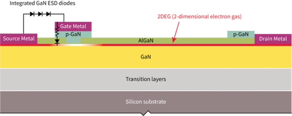
▲그림 1 : 인피니언의 CoolGaN™ GIT 디바이스 단면도
그림 1에서는 또 CoolGaN™ GIT 디바이스의 드레인 금속에 인접한 p-GaN ‘하이브리드 드레인’ 구조를 보여준다.
이 구조는 갇혀 있는 전하를 효과적으로 방출함으로써 RDS(on)이 동적으로 변화되는 것을 완화한다.
다른 업체들의 많은 GaN 트랜지스터 디자인에서 이와 같은 원치 않는 현상이 발생되는 것을 흔히 볼 수 있다.
CoolGaN™ GIT 디바이스의 또 다른 기술적 우위는 더 높은 포화 전류가 가능하다는 것인데, 최대 동작 온도(150℃)에서 특히 그렇다.
그림 2는 70㏁ 정격 CoolGaN™ GIT HEMT 600V와 경쟁사 650V 50㏁ 정격 디바이스의 성능을 비교해서 보여준다.
경쟁사 GaN은 6V의 최대 권장 게이트 전압으로 구동한다고 하더라도 최대 전류가 25A에 불과하다.
이에 비해서 CoolGaN™ 디바이스는 35A의 최대 드레인 전류가 가능하며 전체적인 전류 범위에 걸쳐서 RDS(on)이 더 낮다.
많은 애플리케이션이 일시적인 고전류 조건(스타트업, 라인 사이클 드롭아웃, 낙뢰 스트라이크 등)을 견뎌야 하므로 이와 같은 피크 전류 취급 용량이 중요하다.
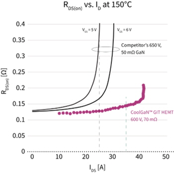
▲그림 2 : 인피니언 CoolGaN™ GIT 디바이스와 경쟁사 디바이스의 성능 비교
이와 같이 견고한 게이트 구조와 높은 피크 전류 취급 용량을 결합함으로써 인피니언의 CoolGaN™은 현재로서 업계에서 가장 견고하고 신뢰할 수 있는 GaN 전력 트랜지스터이다.
■ 시스템 차원의 솔루션
GaN-on-Si 외에도 인피니언은
실리콘 및 실리콘 카바이드(SiC) MOSFET 제품을 제공한다.
전력 반도체 생산에 있어서 이와 같은 포괄적인 접근법은 각기 기술로 어떻게 하면 최상의 성능을 달성할 수 있을지에 대한 깊은 이해를 바탕으로 한다.
CoolGaN™ 제품군은 디스크리트와 IPS(integrated power stage) 제품으로 향상 모드 (normally-off) GIT HEMT 디바이스를 채택해서 전력 변환 애플리케이션의 효율 향상을 이루도록 한다.
이들 디바이스는 훨씬 더 높은 주파수로 스위칭 할 수 있으므로 동작상의 많은 이점을 가져온다.
그런데 기존 패키지 리드는 기생 임피던스로 인해서 이러한 이점들을 반감시킬 수 있다.
이것을 피하기 위해서 인피니언은 CoolGaN™ GIT 디바이스에 쓰루홀 패키징 대신에 SMD(surface mount device) 기술을 사용함으로써 스위칭 속도 이점을 최대한 실현하도록 한다.
여기에서 WBG 반도체의 패키지와 이점에 관해서 더 자세한 정보를 볼 수 있다.
인피니언은 CoolGaN™ GIT 디바이스 시리즈를 지원하기 위해서 절연형 및 비절연형 단일 및 듀얼 채널 제품을 비롯한 일련의
EiceDRIVER™ 게이트 드라이버 IC를 제공한다.
EiceDRIVER™ 1EDi 및
2EDi 제품군은 입력과 출력 채널 사이에 절연을 제공하므로 더 빠른 스위칭과 좀 더 정확한 타이밍을 가능하게 한다.
.jpg)
▲그림 3 : 디스크리트 솔루션에서부터 특정용도 IPS 시스템 솔루션에 이르기까지 포괄적인 솔루션 제공
인피니언은 현장에서 신뢰할 수 있는 동작을 보장하기 위해서 CoolGaN™ GIT 디바이스로 JEDEC 표준에서 정의하고 있는 요건을 상회해서 엄격한
검증 및 신뢰성 테스트 절차를 적용한다.
GaN 디바이스는 비교적 최근에서야 양산이 가능하게 되었다. 그러므로 디바이스 검증을 위해서 산업 표준 방법론을 개발하는 것이 필요하다.
그렇게 해서 품질 보장에 대한 통일된 접근법이 가능해진다면 고객들이 개별 업체들마다 사용하는 절차에 대해서 따로 확인할 필요가 없어진다.
바로 이러한 노력으로서 인피니언은 JEDEC 내에서
GaN 소위원회(JC-70.1)를 창립할 것을 발의하고 그러기 위해서 힘을 보태고 있다. 이 소위원회에서는 GaN 전력 디바이스 검증을 위한 가이드라인과 표준을 개발한다.
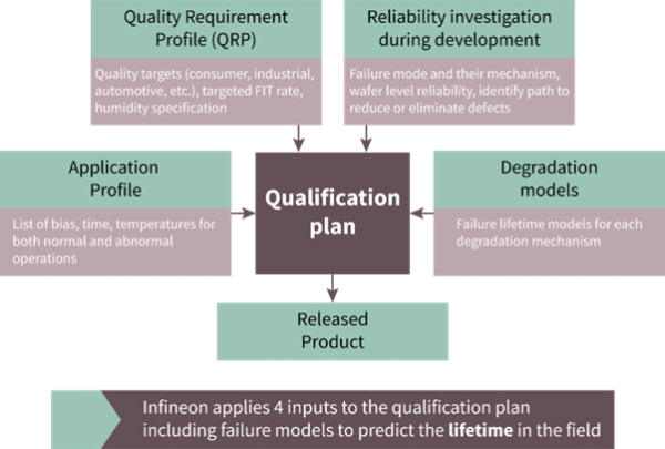
▲그림 4 : CoolGaN™ GIT 디바이스에 대해서 4개 파트로 이루어진 인피니언의 포괄적인 검증 접근법
최근 들어서 와이드 밴드갭 전력 반도체에 대한 수요가 크게 증가하면서 공급이 달리게 되었다.
이에 고객들이, 시장 수요가 계속해서 증가하더라도 고품질의 신뢰할 수 있는 디바이스를 공급 중단 없이 안정적으로 확보하기 위해서 나서고 있다.
인피니언은 세계 최대의 전력 반도체 공급 업체로서 탄탄한 생산 용량을 구축하고 있으며 공급 안정성이 탁월한 것으로 시장에서 인정받고 있다.
GaN 에피택시, 전위 및 후위 공정, 패키징, 테스트 같은 핵심 기술들을 자체적으로 보유함으로써 인피니언은 GaN 디바이스로 공급망에 대한 완벽한 통제권을 쥐고 있다. 이것은 실리콘 제품으로 축적된 경험을 바탕으로 한 것이다.
인피니언은 계속해서 생산 용량을 증설하고 있으며, 최근에는
오스트리아 필라흐 공장에 대대적인 300㎜ 실리콘 제조 설비를 건설하고 가동에 들어갔다.
실리콘 생산을 이 신규 설비로 이전한 다음에는, 기존 150㎜ 및 200㎜ 웨이퍼 생산 라인을 GaN 디바이스 생산으로 돌릴 예정이다.
인피니언의 검증된 할당 관리 프로세스와 함께 이와 같은 생산 용량 증설로 유연성을 높이면서 고객 주문을 극히 효율적으로 처리하게 되었다.
또한 말레이시아 쿨림 공장에 프론트앤드 용량을 추가적으로 확대할 계획이다.
이것은 GaN 에피택시 용량을 추가적으로 늘릴 수 있는 여유를 확보할 것이다.
또한 최근에 인피니언은 이 공장에
3차 생산 모듈을 건설하기 위해서 20억 유로 이상을 투자하기로 결정했다. 그럼으로써 와이드 밴드갭(SiC와 GaN) 반도체 생산 용량을 크게 늘릴 것으로 기대된다.
공급 중단 사태를 방지하기 위해서 인피니언은 모든 비즈니스 프로세스를 아우르는 포괄적인 비즈니스 연속성 관리 프레임워크를 도입하고 있다.
가치 사슬 전반에 걸쳐서 각각의 단계마다 세부적인 위험성 평가를 실시해서 잠재적인 위험을 조기에 파악하고 신속하게 대응하도록 한다.
파급력이나 발생 가능성에 따라서 다양한 상황을 평가 및 분류하고 그에 따라서 적절한 조치들을 취한다.
이 프레임워크는 협력사들까지도 포함한다. 협력사들이 인피니언의 정확한 요건을 충족하는지 평가한다. 그럼으로써 팬데믹, 지정학적 사건, 원자재 부족 같은 예기치 않은 상황 속에서도 공급망 연속성을 보장하도록 한다.
■ 고객 지원
인피니언은 유통 채널들에 대해서 포괄적인 기술 지원을 제공할 뿐만 아니라, 고객들을 위해서
셀프 서비스 설계 지원 플랫폼을 제공한다.
신제품 개발 시에 디바이스 동작과 특징을 설명하기 위해서 상세하고도 정확한 테크니컬 도큐멘테이션을 작성한다.
이러한 것으로서 제품 데이터 시트와 일련의 애플리케이션 노트를 통해서 새로운 디바이스 제품을 어떻게 사용하고 이전 세대 인피니언 제품이나 경쟁사 제품과 비교해서 성능이 어떻게 향상되었는지 설명한다.
또한 인피니언은 많은 제품에 대해서 디바이스 성능을 평가해볼 수 있도록 애플리케이션 보드를 제공한다.
이러한 애플리케이션 보드는 인피니언 웹사이트(온라인
Board Finder)나 유통판매 파트너사들을 통해서 구입할 수 있다.
애플리케이션 보드와 함께, 제품 등록 환경(myInfineon)에서는 스키매틱, 레이아웃, BOM, 펌웨어 같은 것들을 이용할 수 있다.
또한 인피니언은 세계 여러 나라에서 전문적이고 숙련된 필드 애플리케이션 엔지니어 팀을 지원한다.
이들 FAE 팀이 고객들이 문제를 해결할 수 있도록 현지에서 기술적 자문과 지원을 제공한다.
또한 인피니언이 제공하는
온라인 커뮤니티에서는 포럼 활동을 통해서 기술적 정보를 얻고 의견을 나눌 수 있다.
■ 인피니언, 고품질 GaN 제품군 공급
인피니언은 기술적 탁월성과 함께 안정적인 생산 용량을 확보하고, 공급망 관리에 있어서 오랜 기간에 걸쳐서 경험을 축적하고, 포괄적인 비즈니스 연속성 프로세스를 확립함으로써 GaN 전력 디바이스에 대한 수요 증가를 잘 관리하고 고객들에게 고품질의 신뢰할 수 있는 제품을 적시에 공급하기 위해서 만반의 대비를 갖추고 있다.
여기를 클릭하면 인피니언의 효율적이며 신뢰할 수 있는 CoolGaN™ GIT HEMT 기술에 대해서 더 자세히 볼 수 있으며, 스위치, 드라이버, 최근에 출시된
IPS 제품군(CoolGaN™ IPS)을 비롯한 전체적인 시스템 제품 포트폴리오를 볼 수 있다.
※ 기고자
Eric Persson, Senior Principal Engineer, 인피니언 테크놀로지스
.jpg)
.jpg)


