이종 접합(Heterogeneous Integration, HI)은 성능·밀도는 높이고 비용은 줄이는 첨단 솔루션으로, 미세 공정 한계에 따라 반도체 업계는 패키지단에서의 움직임이 활발한 상황이다. 새롭게 출시된 어플라이드의 이종 접합 제조 솔루션은 칩의 PPACt(전력∙성능∙크기∙비용∙시장출시기간)을 개선해 패키지단에서의 무어의 법칙 달성에 기여하고 있다.
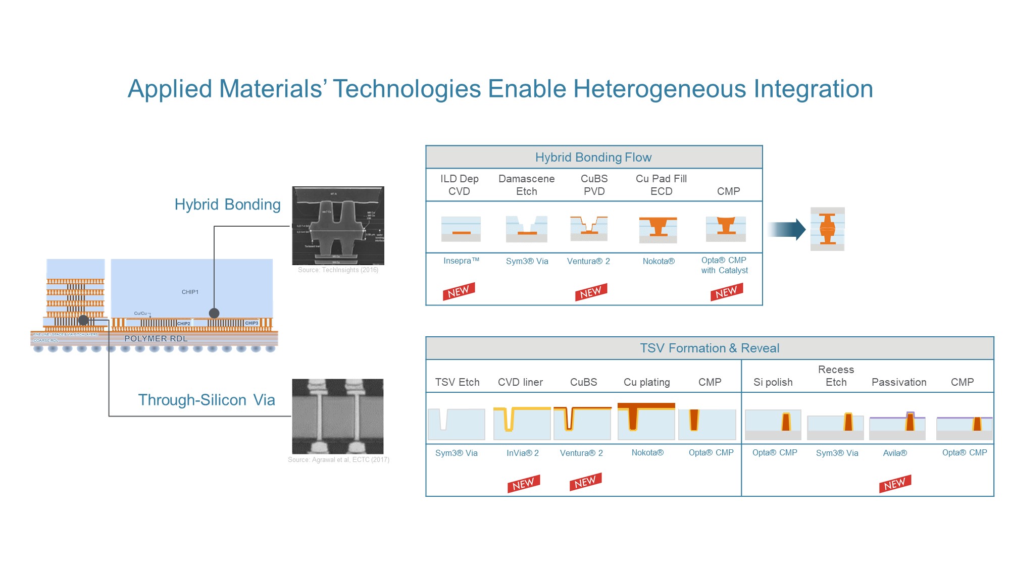
▲ 이종 접합 칩 제조를 위한 어플라이드 신기술
신소재·시스템 통해 본딩 성능·신뢰성 향상
新증착 시스템, 적층 밀도·성능·품질·비용↑
이종 접합(Heterogeneous Integration, HI)은 성능·밀도는 높이고 비용은 줄이는 첨단 솔루션으로, 미세 공정 한계에 따라 반도체 업계는 패키지단에서의 움직임이 활발한 상황이다. 새롭게 출시된 어플라이드의 이종 접합 제조 솔루션은 칩의 PPACt(전력∙성능∙크기∙비용∙시장출시기간)을 개선해 패키지단에서의 무어의 법칙 달성에 기여하고 있다.
재료공학 솔루션 분야 글로벌 선도 기업 어플라이드 머티어리얼즈가 하이브리드 본딩과 실리콘관통전극(TSV∙Through-Silicon Via) 공법을 사용해 칩렛을 최신 2.5D 및 3D 패키지에 통합하는 데 도움이 되는 재료·기술·시스템을 출시했다고 18일 밝혔다.
이종 접합은 반도체 회사가 다양한 △기능 △기술 노드 △크기의 칩렛을 최신 패키지로 결합해 단일 제품처럼 작동하도록 지원한다. 고성능 컴퓨팅, 인공지능(AI) 같은 분야에서 트랜지스터 필요성은 기하급수로 증가하는 반면, 기존 2D 스케일링을 통해 트랜지스터를 축소하는 방식은 느리고 더 많은 비용이 소요된다.
이종 접합은 반도체 제조업체가 새로운 방식으로 칩의 PPACt(전력∙성능∙크기∙비용∙시장출시기간)을 개선하도록 지원하는 새로운 플레이북의 핵심으로 업계에서 크게 주목 받고 있는 상황이다.
어플라이드는 △식각 △물리기상증착(PVD) △화학기상증착(CVD) △전기 도금 △화학기계연마(CMP) △열처리 △표면 처리를 포괄하는 최적화된 칩 제조 시스템을 갖춘 최대 규모 이종 접합 제조 기술 업체다.
순다르 라마무르티(Sundar Ramamurthy) 어플라이드 머티어리얼즈 반도체 제품 그룹의 HI∙ICAPS∙에피택시 부문 부사장 겸 총괄 매니저는 “성능, 전력, 비용을 동시에 개선할 수 없는 기존 2D 미세화의 한계를 극복하는 데 이종 접합 칩기술이 도움되기 때문에 빠르게 성장하고 있다”며 “어플라이드의 최신 HI 솔루션은 2.5D 및 3D 구성에서 더 많은 트랜지스터와 배선을 패키징하는 첨단 기술을 발전시키며, 이를 통해 시스템 성능은 높이면서 전력 소비는 줄이고 크기를 최소화해 시장 출시 시간을 단축할 수 있다”고 말했다.
■ 더 강력한 하이브리드 본딩
칩 투 웨이퍼(chip-to-wafer), 웨이퍼 투 웨이퍼(wafer-to-wafer) 하이브리드 본딩은 직접 구리-구리 결합을 사용해 칩을 연결함으로써 결합된 소자가 단일 제품의 성능을 내도록 한다. 하이브리드 본딩은 현재 가장 발전된 이종 접합 기술로, 더 작은 공간에 더 많은 배선을 집적하고 신호가 이동하는 거리를 줄임으로써 처리량(throughput)과 전력을 개선한다.
어플라이드가 출시한 인세프라(Insepra) SiCN 증착 시스템은 어플라이드가 선도하고 있는 하이브리드 본딩 제품군의 포트폴리오를 확장한다. 이 시스템은 업계 최고 수준의 유전체 본딩 강도를 자랑하며, 우수한 구리 확산 배리어 특성을 제공하는 새로운 실리콘탄소질화물(SiCN) 소재를 사용한다. 강력한 유전체 결합으로 주어진 면적에 훨씬 더 많은 구리-구리 인터커넥트 통합에 필요한 구조적 안정성을 확보함으로써 전력 소비를 낮추고 기기 성능을 높인다.
함께 출시된 카탈리스트(Catalyst) CMP 솔루션을 통해 고객은 후속 고온 열처리 단계에서 결합될 두 표면의 구리 소재를 의도적으로 오목하게 만드는 '디싱(dishing)' 양을 제어할 수 있다. CMP 디싱은 구리 패드의 상단 표면에 원치 않는 금속 손실을 발생시켜 구리-구리 결합의 완성도와 강도를 떨어뜨리는 에어 갭을 유발할 수 있다. 어플라이드의 카탈리스트 솔루션은 디싱을 줄이고 처리량을 높이는 동적 온도 제어 기술이다.
■ 더 높은 종횡비의 TSV
10년 이상 반도체 양산에 사용된 TSV는 적층된 칩을 정밀하게 연결해 주는 수직 와이어다. 실리콘에 트렌치를 식각한 다음 절연박막과 금속 와이어로 채우는 방식이다. 많은 로직, 메모리, 특수 칩이 최신2.5D 및 3D 패키지에 통합됨에 따라 TSV 인터커넥트 수가 패키지당 수백 개에서 수천 개로 확장되고 있다. 더 많은 인터커넥트를 통합하고 더 높은 칩 스택을 수용하기 위해 비아를 더 좁고 높게 만들어야 하는데, 이는 증착 균일성을 저하시켜 성능이 저하되고 저항과 전력 소비는 증가시키게 된다.
어플라이드는 더 높은 종횡비의 TSV를 구현하고 반도체 제조업체가 통합, 성능, 전력 목표를 달성하도록 지원하는 유전체와 금속 증착을 위한 새로운 기술을 선보였다.
프로듀서 인비아2(Producer InVia 2) CVD 시스템은 다양해지는 TSV 응용 분야에서 로직 및 메모리 고객이 필요한 극한의 종횡비에서 유전체 라이너를 균일하고 전기적으로 견고하게 만드는 새로운 CVD 공정이다. 인비아 2 시스템은 특수 인 시튜(in-situ) 증착 공정을 사용해 고종횡비 TSV에 탁월한 적합성을 제공한다. 원자층증착(ALD) 기술보다 높은 생산성을 제공함으로써 TSV의 웨이퍼당 비용을 절감시켜 도입이 더욱 확대될 수 있다.
엔듀라 벤튜라2(Endura Ventura 2) PVD 시스템은 널리 채택된 기존 제품을 최대 20:1 종횡비를 가진 TSV 응용 분야로 확장한 제품이다. 벤튜라2 시스템은 높은 전기적 성능과 신뢰성을 제공하는 완전한 필링을 위해 금속 TSV 와이어 증착의 제어를 향상시킨다.
새로운 TSV PVD 공정은 프로듀서 인비아 2 CVD 공정과 함께 사용하도록 최적화돼 고객에게 가장 까다로운 TSV 설계에 대해 준비된 솔루션을 제공한다. 벤튜라2 시스템은 모든 첨단 파운드리 및 로직 칩 제조업체와 모든 주요 D램 생산업체가 사용 중이다.
어플라이드의 최신 프로듀서 아빌라(Producer Avila) PECVD 시스템은 TSV ‘리빌(reveal)’ 애플리케이션을 위해 설계됐다. TSV 공정 흐름에서 웨이퍼는 임시로 유리 또는 실리콘 캐리어에 접착된 다음 CMP와 식각을 사용해 얇게 만들어 TSV를 사용하도록 한다.
TSV 리빌 단계에 이어 플라즈마CVD 기술을 사용해 TSV를 전기적으로 분리하는 얇은 유전체 층을 증착한다. PECVD 공정에서 섭씨 약 200도 이상의 열이 발생하면 섬세한 임시 본딩이 손상돼 웨이퍼 수율 손실이 발생할 수 있다. 어플라이드 프로듀서 아빌라PECVD 시스템은 초저온에서 고속으로 고품질 유전막을 생성해 TSV 품질과 비용에 필요한 낮은 열 예산과 높은 생산성을 제공한다.
새롭게 출시된 어플라이드 솔루션 및 시스템에 대한 자세한 정보는 어플라이드 웹사이트에서 확인할 수 있다.