ETRI, 95% 절전 반도체 패키징 원천기술 개발
기사입력 2023.07.28 13:24
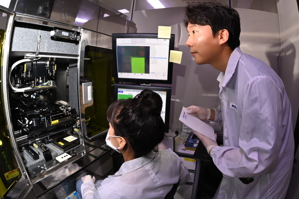
▲ETRI 연구진이 칩렛 집적 공정에 대해 논의하는 모습(좌측부터 이찬미 연구원, 최광문 선임연구원)
기존 9단계 공정 3단계로 줄여, 필름 신소재 첫 개발
공정성·신뢰성 평가 중 향후 3년내 상용화 가능 전망
공정성·신뢰성 평가 중 향후 3년내 상용화 가능 전망
국내 연구진이 최첨단 반도체 개발의 키를 쥐고 있는 패키징(Packaging) 분야의 핵심원천 신소재 기술개발에 성공, 반도체강국의 신화를 계속 써 나가는데 청신호가 켜졌다.
향후 본 기술은 자율주행, 데이터센터 등 고성능이 필요한 AI반도체 제조의 핵심 소재기술로 사용될 전망이다.
한국전자통신연구원(ETRI)은 자체 보유한 나노 소재기술을 이용해 세계최초로 반도체 공정에 꼭 필요한 신소재를 개발해 냈다.
특히 본 기술은 기존 일본이 보유한 기술 대비 95% 전력 절감이 가능한 획기적인 반도체 칩렛 패키징 기술이다.
공정단계도 기존 9단계를 3단계로 대폭 줄였다.
연구진이 개발한 95% 절전 첨단 반도체 칩렛 패키징 기술은 반도체 웨이퍼에 연구원이 개발한 신소재인 비전도성 필름(NCF)을 붙인 후 타일처럼 생긴 칩렛에 면 레이저를 조사(照射)해 경화하는 총 3단계로 이뤄진다.
그동안 반도체 업계에서는 첨단 반도체 패키징 공정에 주로 일본 소재를 사용해 왔다.
반면에 공정이 총 9단계를 거치는 등 복잡하고 다양한 장비가 사용되며 높은 전력소모, 청정실 유지비용, 유해물질 배출 등이 큰 단점이었다.
아울러 대만반도체제조회사(TSMC), 인텔, 삼성전자 등 글로벌 반도체 기업들이 수 나노미터(㎚)의 첨단 반도체 선단으로 만들어진 고밀도 칩을 위한 새로운 집적 기술개발에 박차를 가하고 있다.
기존기술로는 칩렛 집적기술이 요구하는 수십 마이크로미터(㎛) 크기의 칩간 연결통로라 할 수 있는 접합부의 세척 불가능, 상온에서 접합의 필요성 등이 적용하기 어렵다는 단점도 있었다.
연구진이 개발한 기술은 자체 보유한 나노소재 설계기술과 나노신소재를 활용해 20여년 핵심원천기술 연구 끝에 독자 개발해 냈다.
개발한 공정은 첨단 반도체 웨이퍼 기판에 개발한 나노 신소재를 적용한 후 다양한 웨이퍼에서 제작된 칩렛으로 타일을 만들어 1초 정도의 면 레이저를 쏘아서 접합 공정을 완성하고 후경화 공정으로 완료된다.
연구진이 개발에 성공한 핵심 신소재는 고분자 필름으로 만들었다.
10∼20㎛두께의 에폭시 계열 소재에 환원제 등이 첨가된 나노소재다.
본 소재에 레이저를 쏘면 반도체 후공정(패키징)의 단계에서 세척, 건조, 도포, 경화 등에 이르는 전 단계를 해결한다.
따라서 ETRI가 개발에 성공한 본 나노 신소재는 소재가 갖는 특수성으로 인해 반도체 후공정에 필요한 접합소재 역할과 각 단계에 이르는 소재 특징을 갖고 있는 셈이다.
아울러 기존에는 웨이퍼에서 분리한 칩을 보드에 붙여 한 개씩 잘라서 쓰는 방식이었다.
이런 방식도 연구진의 나노 신소재 덕분에 칩렛을 웨이퍼 기판에 마치 타일을 붙이듯 직접 찍어 붙이는 게 가능해졌다.
이처럼, 본 기술은 공정이 간단해 전체 생산라인을 기존 20미터(M)이상을 4미터로 즉, 20%로 줄일 수 있다.
질소 가스도 필요 없어 유해물질이 발생하지 않는 장점도 있다.
첨단 칩렛 패키지에 적용할 수 있는 고정밀 공정이라는 특징도 아울러 있다.
특히 고정밀 공정을 개발하기 위해 세계 최초로 상온(25℃)에서 집적 공정이 가능하다는 것이 특징이다.
기존 공정들은 모두 스테이지 온도를 100℃로 가열해 전력 소모는 물론 열팽창으로 인한 오차 증가, 신뢰성 저하의 문제를 가지고 있었다.
ETRI 연구진은 특성 온도 변화 이상에서 활성화되는 나노 소재 설계 기술을 이용하여 온도 상승으로 인한 흄(연기) 발생 없이 상온 스테이지에서도 접합 공정이 가능한 신소재와 신공법을 세계 처음으로 개발해 냈다고 설명했다.
특히 본 기술은 미국의 마이크로 LED 관련 스타트업은 물론 첨단 반도체 분야의 세계적인 파운드리 회사가 공정성과 신뢰성 평가를 진행하고 있어 향후 우수 평가시 3년 내 상용화가 가능할 것으로 전망하고 있다.
ETRI 연구진은 향후, 반도체 디스플레이 업체가 필요로 하는 저전력·친환경 공법에 본 기술이 해답을 제공할 수 있을 것으로 판단했다.
첨단 칩렛 집적과 마이크로 LED 전사·접합 공정에 적용해 기술의 확장성과 응용성을 확대할 계획이다.
ETRI 이일민 창의원천연구본부장은 “최근 ESG 경영이 반도체 디스플레이 업계의 화두이고 산업계에 친화적인 저전력 신공법을 누가 먼저 개발하느냐가 사활이 걸린 문제로 본 기술은 파급효과가 매우 큰 기술”이라고 말했다.
ETRI 최광성 실장도 “그동안 첨단 반도체 패키징과 마이크로 LED 디스플레이 분야는 일본 소재와 장비 기술에 대한 의존도가 높았다. 기술 격차가 커서 자립화가 쉽지 않는 상황이었는데 저전력, 친환경이라는 새로운 시장의 요구에 연구진의 성과가 답해 원천기술의 상용화가 기대된다”고 밝혔다.
세계적 시장조사기관인 욜 디벨롭먼트에 따르면, 2027년 칩렛 패키징 시장 관련 시장규모는 239억불로 예측하고 있다.
본 연구는 과학기술정보통신부 ‘소재혁신선도 프로젝트’의 지원으로 연구 중이며, 소재혁신선도 프로젝트에는 KIST, 한국세라믹기술원, 한국생산기술연구원이 공동연구기관으로 참여 중이다.
연구진은 세계 최대 디스플레이 학회인 ‘2023 SID 디스플레이 위크’에서 최신기술논문으로 선정됐고 세계 최대 첨단 반도체 패키징 학회인 ‘2023 IEEE ECTC’ 학술대회에서 본 성과를 발표해 우수성을 인정받았다.
연구진은 지난 2021년, 세계최초 LED 전사·접합 공정을 하나로 만든 사이트랩(SITRAB) 신소재 기술을 개발, 관련 기업과 활발히 기술이전 협상을 진행중이다.
ETRI는 동시 전사-접합 기술 및 레이저에 신소재를 적용한 공정 기술과 소재 관련 연구를 통해 SCI 논문과 국내·외 특허 출원 및 등록 23건 성과를 얻었다.
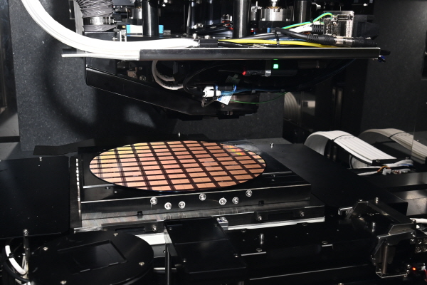
▲면 레이저를 통한 칩렛 칩적 공정 수행 모습


.png)

관련 웨비나


많이 본 뉴스
[열린보도원칙] 당 매체는 독자와 취재원 등 뉴스이용자의 권리 보장을 위해 반론이나 정정보도, 추후보도를 요청할 수 있는 창구를 열어두고 있음을 알려드립니다.
고충처리인 장은성 070-4699-5321 , news@e4ds.com