마드후라 탑세 ADI 선임 스태프 엔지니어가 디바이스 전원 공급 IC를 선택할 때 중요하게 고려해야 할 두 가지 사항에 대해 설명한다.
“디바이스 전원 공급 IC, 범위 전환 글리치 고려 必”
낮은 전류 범위로 전환 시 글리치 발생, DUT 손상 가능성
MAX32010, 글리치 미발생 범위 전환 가능·테스트 신뢰도 ↑
이 글에서는 디바이스 전원 공급 IC를 선택할 때 중요하게 고려해야 할 두 가지 사항인 범위 전환 글리치(range change glitch)와 전원 공급 효율, 그리고 특정 애플리케이션의 요구 사항에 맞게 DPS 시스템을 설계하는 방법에 대해 설명한다.
자동화 테스트 장비(automated test equipment, ATE)에서 디바이스 전원 공급(device power supply, DPS) IC를 사용하면 테스트 요구사항에 따라 유연하게 FV(force voltage) 및 FI(force current)를 공급할 수 있다.
부하 전류가 설정된 두 개의 전류 한계 사이에 있다면 DPS IC는 전압 소스로 동작하고, 설정된 전류 한계에 도달하면 매끄럽게 정밀 전류 소스/싱크로 전환한다.
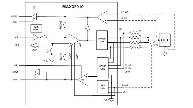
▲그림 1. MAX32010 다이어그램
그림 1은 아나로그디바이스의 차세대 디바이스 전원 공급 IC인 MAX32010의 아키텍처를 보여준다.
FIMODE, FVMODE, FISLAVE MODE 스위치는 FV, FI, FI Slave 모드를 선택하고, HIZF 및 HIZM 스위치는 각각 MV(measure voltage) 및 MI(measure current) 모드를 선택한다.
RANGE MUX는 외부 검출 저항과 함께 작동해서 서로 다른 전류 범위(RA(1.2A), RB(20mA), RC(2mA), RD(200mA))를 가능하게 한다.
공식 RSENSE = 1V/IOUT에 따라 검출 저항 값을 변경해서 특정한 전류 범위를 설정할 수 있다. CLEN 스위치와 ICLMP 및 VCLMP DAC를 사용해서 전압 및 전류 클램프를 설정할 수 있다.
■ 범위 전환 글리치
첫 번째 고려사항인 범위 전환 글리치를 살펴보면 ATE가 DUT 테스트를 하는 동안 시스템이 다른 테스트로 전환하기 위해 전류 범위를 바꿔야 할 때가 있다.
IDDQ, 즉 대기 전류(quiescent current) 측정은 작은 값의 전류를 측정하기 위해서 통상적으로 매우 낮은 전류 범위를 필요로 한다.
이 때 극히 낮은 전류 범위로 전환하면 전압 스파이크 혹은 글리치가 발생하여 측정에 영향을 미칠 뿐만 아니라 DUT를 손상시킬 수 있다.
글리치를 일으키지 않는 범위 전환은 DUT를 보호하고 테스트의 신뢰도를 높일 수 있다.
그림 2에서는 270pF의 부하 커패시터를 사용하여 테스트했을 때 ADI의 DPS IC가 어떠한 글리치도 일으키지 않으면서 아주 매끄럽게 전환한다는 것을 알 수 있다.
부하 커패시터를 사용하지 않을 경우(0pF), 이 전환은 25mV/20ms의 램프 레이트로 20ms 동안 일어난다.
이는 경쟁사 제품의 글리치보다 훨씬 작은 것이다.
경쟁사 제품은 수 마이크로초 동안 159mV의 글리치를 나타낸다.
따라서 ADI의 DPS IC 성능이 경쟁사 제품의 범위 전환 성능보다 536% 더 우수하고, DUT에 어떠한 손상도 일으키지 않는다는 것을 알 수 있다.
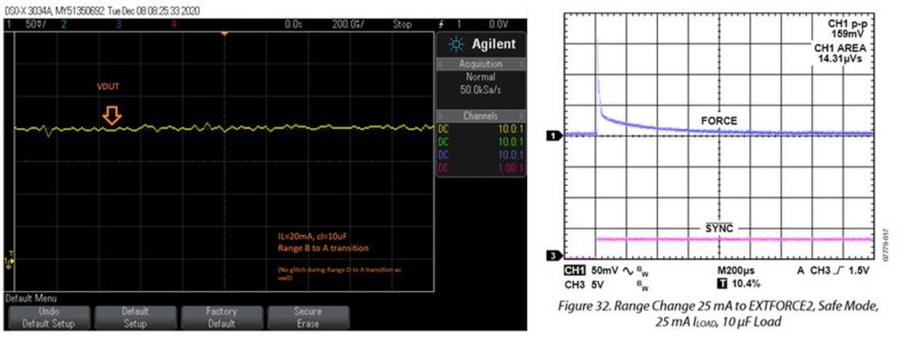 ▲
▲그림 2. 아나로그디바이스의 제품과 경쟁사 제품의 범위 전환 글리치 비교
■ 디바이스 전원 공급 효율
DPS IC를 선택할 때 또 다른 중요한 고려사항은 디바이스 전원 공급 효율이다.
이 효율이 비용 절감과 시스템 신뢰성에 직접적으로 영향을 미치기 때문이다.
효율이 높을수록 비용 절감 효과와 신뢰성이 우수하고, 시스템 수명 또한 연장한다.
DPS 효율이 떨어질수록 더 많은 열을 발생하고, 더 많은 열 발생은 부품을 더 빨리 마모시키고 더 자주 고장을 일으킨다.
DPS 효율은 ‘효율 = 출력 전력/입력 전력’으로 계산할 수 있다.
표 1에서 보듯이, ADI 제품은 경쟁사 제품보다 높은 효율(58.33%)로 더 높은 전류(1.2A)를 제공한다.
ADI의 DPS 효율은 경쟁사 2의 DPS IC보다는 11% 더 우수하고 경쟁사 1보다는 155% 더 우수하다.
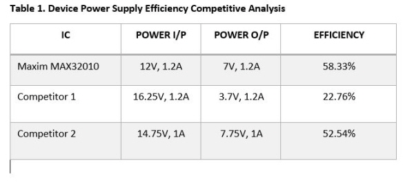
▲표 1. 디바이스 전원 공급 효율 비교
■ 특정한 부하 전류 요구를 충족하도록 DPS를 설계하는 방법
이번에는 특정 애플리케이션의 요구 사항을 충족하는 DPS 시스템을 설계할 때 몇 가지 고려 사항에 대해 알아본다.
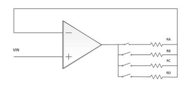
▲그림 3. 검출 저항을 사용해서 특정한 부하 전류 선택
각각의 ATE는 테스트하고자 하는 디바이스(DUT)에 따라서 특정한 부하 전류 요구 사항을 갖는다.
MAX32010은 단 하나의 검출 저항 값만 변경해서 특정한 범위를 선택할 수 있다.
MAX32010의 RANGE MUX는 RA(1.2A), RB(20mA), RC(2mA), RD(200mA) 전류 범위 중의 하나를 선택한다.
공식 RSENSE = 1V/IOUT에 따라서 검출 저항 값을 선택할 수 있다.
만약 필요한 부하 전류가 5mA라고 한다면, 5mA는 범위 B에 해당된다.
적절한 RSENSE를 선택하고자 한다면 RSENSE = RB = 1V/5mA = 200Ω이다. ADI의 애플리케이션 노트 7068에서는 검출 저항 선택과 관련한 보다 자세한 설명을 제공한다.
■ 더 높은 출력 전류를 달성하는 방법
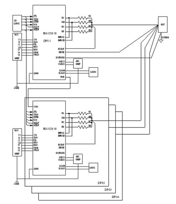
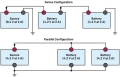
▲그림 4. 병렬 DPS 구성으로 더 높은 출력 전류 달성
DUT는 DPS가 제공할 수 있는 것보다 더 높은 전류를 필요로 할 때가 종종 있다.
그림 4에서 보듯이, 여러 DPS 디바이스를 병렬로 연결함으로써 1.2A 이상의 전류를 제공할 수 있다. 전류를 두 배로 높이기 위해서는 두 개의 디바이스를 모두 FI 모드로 설정한다.
예를 들어, 2개의 7V 1.2A 디바이스를 병렬로 연결하면 최대 7V로 2.4A의 출력 전류를 달성할 수 있다.
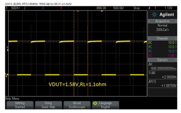
▲그림 5. MAX32010의 50% 듀티 사이클 펄스형 테스트 출력
DPS의 출력 구동 전류를 높일 수 있는 또 다른 방법은 출력을 펄싱하는 것이다.
짧은 지속시간 동안만 전류를 필요로 할 때 그림 5에서 보는 것과 같이 펄스를 사용한 테스트가 가능하다.
이러한 테스트의 한 예가 DUT의 I-V 특성분석이다. 펄스형 테스트를 위해서는 FI 온 시간(On time)의 듀티 사이클을 조절해야 한다.
이 예시의 경우에는 DPS 모드를 50%의 시간에는 FI 모드로 설정하고 나머지 50%의 시간에는 ‘높은 임피던스’ 모드로 설정하고 있다.
듀티 사이클은 DUT의 전류 요구에 따라 조절할 수 있다. MAX32010 IC로 이 시험을 실시했을 때 결과는 최대 출력 전류 = 최대 50% 듀티 사이클로 1.436A다.
■ DPS 시스템에 적합한 히트싱크 선택 방법
신뢰할 수 있고, 안정적인 시스템을 달성하기 위해서는 히트싱크를 잘 선택하는 것 역시 중요하다.
다음 보기에서는 MAX32010을 예로 들어서 적합한 히트싱크를 선택하는 방법을 단계별로 설명한다.
1단계: 패키지 규격을 확인한다. 적합한 히트싱크 선택에는 패키지 열 분석이 유용하다. 열을 소산하기 위한 노출 패드 면적을 아는 것이 중요하다.
2단계: PCB 열 특성을 확인해서 JA의 경계 조건을 계산한다. 전력 손실을 계산하고 열 소산을 위한 모든 매질(전도, 대류, 복사)을 고려한다.
3단계: 패키지 온도 분포를 계산할 때 중요한 두 가지 변수는 히트싱크 베이스 면적과 히트싱크 팬의 유량이다. 이 IC의 접합부 온도를 열 셧다운 온도 아래로 유지하도록 해야 한다. 정지 공기를 사용한 분석 결과를 보면, MAX32010으로 접합부 온도를 140°C 이하로 유지하기 위해서는 베이스 면적 30.48mm x 30.48, 두께 5mm, 핀 길이 15mm인 히트싱크가 필요한 것으로 확인된다(그림 6).
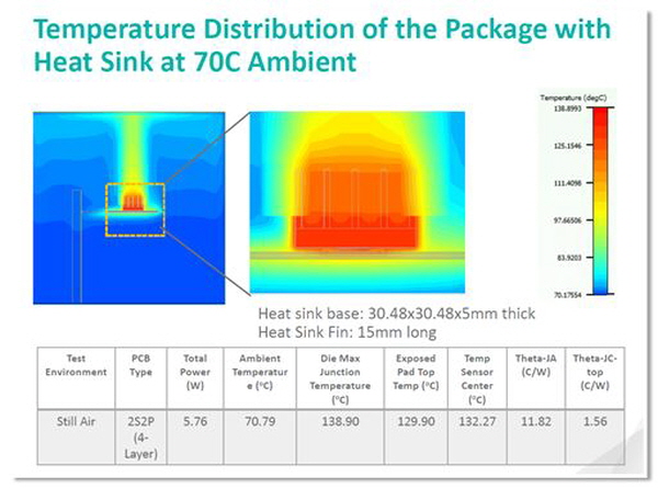
▲그림 6. 히트싱크를 사용했을 때 MAX32010 패키지의 온도 분포
4단계: 이 IC의 접합부 온도를 140C 이하로 유지하는 데에는 공기 흐름과 히트싱크 소재 역시 중요한 역할을 한다. 분석 결과를 보면, 구리 히트싱크에 1m/s의 공기 흐름을 추가함으로써 온도 성능을 크게 향상시킬 수 있는 것으로 나타난다.
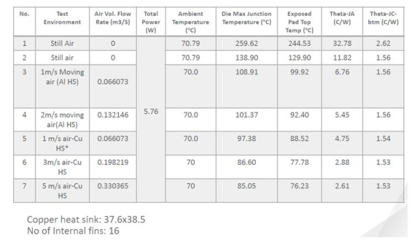
▲그림 7. MAX32010의 열 분석
■ 맺음말
이 글에서는 자동화 테스트 장비(ATE) 시스템에 디바이스 전원 공급(DPS) IC를 선택하는 것과 함께 ATE 시스템의 출력 전류 및 열 요구를 충족하기 위한 시스템 차원의 아키텍처에 대해서도 살펴보았다.
이 글에서 제시한 사항들을 고려해서 특정한 ATE 시스템의 필요에 적합한 DPS IC를 선택할 수 있다.
※ 저자 소개
마드후라 탑세(Madhura Tapse)는 2016년에 MTS(member of technical staff)로 맥심 인터그레이티드(Maxim Integrated, 현재 아나로그디바이스)에 입사했으며, 그 동안에 감시 IC, 전원 모니터링 IC, 인터페이스 IC, ATE IC를 비롯한 다양한 제품군을 담당했다. 그 전에는 사이프레스 세미컨덕터(Cypress Semiconductors)에서 애플리케이션 엔지니어로 근무했다. 인도의 푸네 대학에서 전기공학 학사학위 및 인도 공과대학 – 봄베이에서 생의학 공학 석사학위를 취득했다.