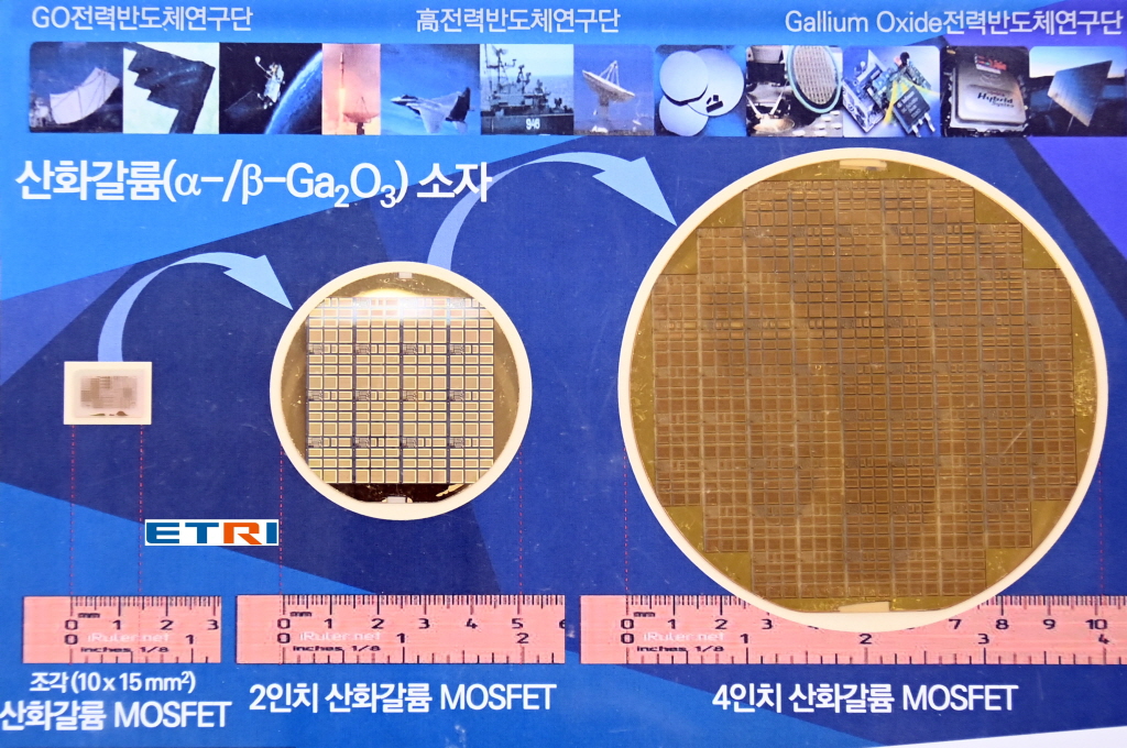
한국전자통신연구원(ETRI)과 한국세라믹기술원(KICET)이 함께 국내 최초로 3kV급 산화갈륨 전력반도체 금속 산화막 반도체 전계효과 트랜지스터(모스펫, MOSFET) 소자 기술을 개발했다.
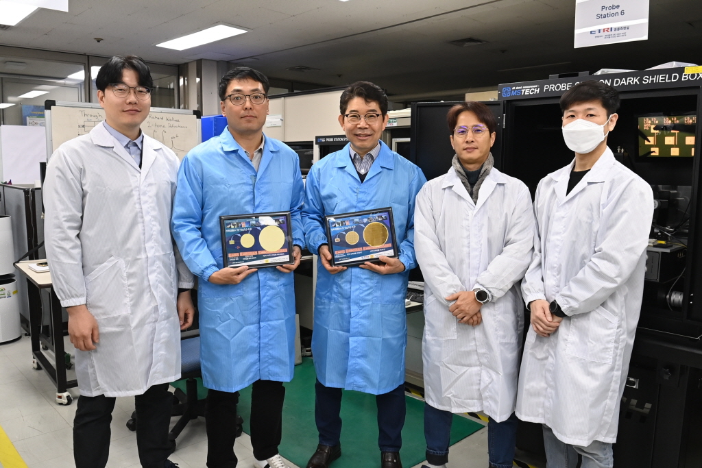
▲Joint research team of ETRI and KICET on gallium oxide epitaxial material and MOSFET devices
Development of next-generation power semiconductor core technology, escaping dependence on foreign countries
Half the size of the device, 10 times the performance, and 20 times the price competitiveness
A domestic research team has succeeded in developing key materials and component process technology for gallium oxide (Ga2O3) power semiconductors, known as the next-generation power semiconductors.
The Electronics and Telecommunications Research Institute (ETRI) announced on the 1st that it, together with the Korea Institute of Ceramic Technology (KICET), has developed the first 3kV gallium oxide power semiconductor metal oxide semiconductor field effect transistor (MOSFET) device technology in Korea.
The gallium oxide epitaxial material technology that the research team successfully developed is a process for growing multiple layers of high-quality conductive thin films on a single crystal substrate.
Dr. Jeon Dae-woo's research team at the Korea Institute of Ceramic Engineering and Technology has succeeded in localizing the growth technology for high-quality beta gallium oxide epitaxial materials using metal-organic chemical vapor deposition (MOCVD), which is expected to be a global technology for mass producing large-diameter epitaxial materials.
This technology can freely create the thickness of epitaxial materials from nanometers (nm), which are one billionth of a meter, to micrometers (㎛), which are one millionth of a meter.
The electron concentration can also be controlled over a wide range.
This makes it easier to develop power semiconductor devices with various voltage and current performances, bringing us closer to mass production technology.
In addition, the research team is developing additional The successful gallium oxide device process technology is a wafer-scale integration process technology that manufactures power semiconductor devices through micro-pattern formation, low-damage etching, deposition, and heat treatment processes on an epitaxial material substrate.
The research team led by Dr. Jae-Kyung Moon of ETRI has developed a 3kV MOSFET device with superior performance by using epi-materials developed directly by the KICET research team rather than commercial overseas epi-materials.
First, we developed a new epitaxial structure that can reduce leakage current to the picoampere (pA, one trillionth of an A) level.
This is the result of newly developing components and process technologies that can significantly improve the breakdown voltage to over 3kV.
This localization of gallium oxide power semiconductor technology is a very important technology for enhancing next-generation global competitiveness and preempting new markets in a situation where most wide bandgap (WBG) power semiconductor technologies, such as gallium nitride (GaN) and silicon carbide (SiC), are currently dependent on foreign countries.
The research team explained that this gallium oxide epitaxial material and power semiconductor MOSFET device technology can reduce manufacturing costs by 1/3 to 1/5 of the existing power semiconductors, and that through local production, Korea will be able to secure leadership in the next-generation power semiconductor high value-added industry.
In addition, gallium oxide semiconductors have superior physical properties and can withstand higher voltages, which allows power semiconductor devices to be miniaturized by up to 50%, while also increasing power conversion efficiency.
Therefore, the performance of power semiconductor devices can be improved by more than 10 times, and the price competitiveness of the devices can be increased by more than 20 times compared to existing power semiconductor devices.
The research team explained that gallium oxide power semiconductor devices can increase power conversion efficiency while reducing the size of inverter and converter systems by more than 1/10.
Future power transmissionIf applied to industrial fields that use a lot of electricity, such as prospects, high-speed railways, data centers, quantum computers, and electric vehicles, the energy saving effect is expected to be significant.
ETRI is focusing on the development of the world's first 4-inch gallium oxide power semiconductor MOSFET device process and commercialization technology using a 4-micron thick plating process.
Accordingly, it seems possible to secure mass production technology for gallium oxide power semiconductors using 4-inch large-area epitaxial materials and device process technologies developed domestically in the future.
According to a 2023 announcement by Japan's Yano Research Institute, the global power semiconductor market is expected to grow to approximately 49 trillion won in 2030, and the gallium oxide market is expected to grow to 1.7 trillion won.
Daewoo Jeon, a senior researcher at the Korea Institute of Ceramic Engineering and Technology, said, “Domestic production of gallium oxide epitaxial material, a key material for next-generation power semiconductors, will enable cost reduction and material independence of epitaxial material, which accounts for more than 40% of the manufacturing cost of domestic power semiconductors.”
ETRI Project Manager Jae-kyung Moon also said, “I think it will further advance the timing of applying gallium oxide power semiconductors to systems. “We plan to commercialize the world’s first multi-kV gallium oxide power semiconductor MOSFET device,” the company said.
This research result was achieved through the 'Development of Key Material Technology for High-Efficiency Ultra-Small Power Semiconductor of Several kV Classes' project, which was carried out as part of the National Core Material Research Group Platform Project of the Nano and Material Technology Development Project of the Ministry of Science and ICT in 2020.

▲Joint research team of ETRI and KICET on gallium oxide epitaxial material and MOSFET devices