기사입력 2024.07.11 14:53

세계적인 반도체 EDA툴 기업 케이던스는 반도체 설계부터 패키징, 검증에 사용되는 SW 솔루션을 제공한다. 케이던스의 AI 기반 EDA 툴은 첨단 노드 및 3D를 지원해 반도체 설계부터 제조, 패키징, 검증 등 최적화 프로세스를 수행한다. 이날 폴 커닝햄 부사장은 EDA를 넘어 컴퓨팅 소프트웨어의 중요성을 강조했다.
2023-09-06 오전 9:58:31by 김예지 기자
케이던스 디자인 시스템즈(Cadence Design Systems, Inc.)는 삼성 파운드리가 ‘케이던스 퀀터스 엑스트랙션(Cadence Quantus Extraction) 솔루션’과 ‘템퍼스 타이밍(Tempus Timing) 솔루션’을 활용해 삼성 5LPE 기술을 바탕으로 한 5G 네트워킹 SoC의 테이프아웃(Tape-out: 설계를 마치고 공정으로 넘어가는 단계)에 성공했다고 12일 밝혔다.
2024-01-12 오후 1:42:09by 김예지 기자
.jpg)
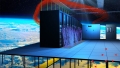
케이던스 디자인 시스템즈(Cadence Design Systems, Inc.)는 5일 업계 최초로 디지털 트윈의 다중물리(Multi-physics) 시스템 설계 및 분석을 가속화할 수 있는 HW/SW 솔루션 ‘케이던스 밀레니엄 엔터프라이즈 다중물리 플랫폼(Cadence Millennium Enterprise Multiphysics Platform)’을 발표했다.
2024-02-06 오전 9:28:38by 김예지 기자
.jpg)
다쏘시스템은 20일 미국 달라스에서 열린 3D익스피리언스 월드 2024에서 케이던스(Cadence Design Systems, Inc)와 솔리드웍스 활용 고객과 미래 고객을 위해 AI기반 케이던스 오아캐드 X(Cadence® OrCAD® X )와 알레그로 X(Allegro® X)를 다쏘시스템 3D익스피리언스 웍스와 통합하여 전략적 파트너십을 지속 확대한다고 밝혔다.
2024-02-20 오후 5:03:10by 김예지 기자
케이던스 디자인 시스템즈(Cadence Design Systems, Inc.)는 지속 가능한 데이터센터 설계와 최신화를 촉진해주는 ‘종합 AI-기반 디지털 트윈 솔루션’을 출시했다고 2일 밝혔다.
2024-04-02 오후 12:20:20by 김예지 기자

[열린보도원칙] 당 매체는 독자와 취재원 등 뉴스이용자의 권리 보장을 위해 반론이나 정정보도, 추후보도를 요청할 수 있는 창구를 열어두고 있음을 알려드립니다.
고충처리인 장은성 070-4699-5321 , news@e4ds.com